 | ÐлекÑÑоннÑй компоненÑ: IRL3103D2 | СкаÑаÑÑ:  PDF PDF  ZIP ZIP |
Äîêóìåíòàöèÿ è îïèñàíèÿ www.docs.chipfind.ru
IRL3103D2
PRELIMINARY
PD 9.1660
7/16/97
Description
The FETKY family of copackaged HEXFET power
MOSFETs and Schottky Diodes offer the designer an
innovative board space saving solution for switching
regulator applications. A low on resistance Gen 5
MOSFET with a low forward voltage drop Schottky
diode and minimized component interconnect
inductance and resistance result in maximized
converter efficiencies.
The TO-220 package is universally preferred for all
commercial-industrial applications at power dissipation
levels to approximately 50 watts. The low thermal
resistance and low package cost of the TO-220
contribute to its wide acceptance throughout the
industry.
l
Copackaged HEXFET
®
Power MOSFET
and Schottky Diode
l
Generation 5 Technology
l
Logic Level Gate Drive
l
Minimize Circuit Inductance
l
Ideal For Synchronous Regulator Application
Parameter
Max.
Units
I
D
@ T
C
= 25°C
Continuous Drain Current, V
GS
@ 10V
54
I
D
@ T
C
= 100°C
Continuous Drain Current, V
GS
@ 10V
34
A
I
DM
Pulsed Drain Current
220
P
D
@T
A
= 25°C
Power Dissipation
2.0
W
P
D
@T
C
= 25°C
Power Dissipation
70
W
Linear Derating Factor
0.56
W/°C
V
GS
Gate-to-Source Voltage
± 16
V
T
J
Operating Junction and
-55 to + 150
T
STG
Storage Temperature Range
Soldering Temperature, for 10 seconds
300 (1.6mm from case )
Mounting torque, 6-32 or M3 srew
10 lbf·in (1.1N·m)
°C
Absolute Maximum Ratings
V
DSS
= 30V
R
DS(on)
= 0.014
I
D
= 54A
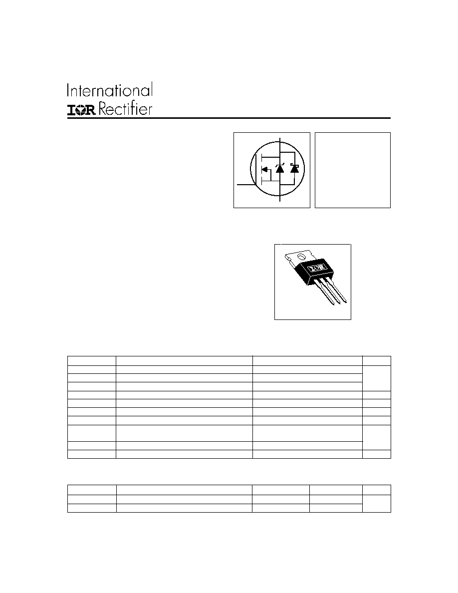
FETKY
TM
MOSFET & SCHOTTKY RECTIFIER
Parameter
Typ.
Max.
Units
R
JC
Junction-to-Case
1.8
R
JA
Junction-to-Ambient
62
°C/W
Thermal Resistance
G
D
S
TO-220AB
IRL3103D2
Parameter
Min. Typ. Max. Units
Conditions
I
F
(AV)
( Schottky)
MOSFET symbol
showing the
I
SM
Pulsed Source Current
integral reverse
(Body Diode)
p-n junction and Schottky diode.
V
SD1
Diode Forward Voltage
1.3
V
T
J
= 25°C, I
S
= 32A, V
GS
= 0V
V
SD2
Diode Forward Voltage
0.6
V
T
J
= 25°C, I
S
= 3.0A, V
GS
= 0V
t
rr
Reverse Recovery Time
51
77
ns
T
J
= 25°C, I
F
= 32A
Q
rr
Reverse Recovery Charge
47
71
nC
di/dt = 100A/µs
t
on
Forward Turn-On Time
Intrinsic turn-on time is negligible (turn-on is dominated by L
S
+L
D
)
Repetitive rating; pulse width limited by
max. junction temperature. ( See fig. 10 )
Notes:
Pulse width
300µs; duty cycle
2%.
Uses IRL3103 data and test conditions
Body Diode & Schottky Diode Ratings and Characteristics
5.0
220
A
Parameter
Min. Typ. Max. Units
Conditions
V
(BR)DSS
Drain-to-Source Breakdown Voltage
30
V
V
GS
= 0V, I
D
= 250µA
V
(BR)DSS
/
T
J
Breakdown Voltage Temp. Coefficient
0.037
V/°C
Reference to 25°C, I
D
= 1mA
0.014
V
GS
= 10V, I
D
= 32A
0.019
V
GS
= 4.5V, I
D
= 27A
V
GS(th)
Gate Threshold Voltage
1.0
V
V
DS
= V
GS
, I
D
= 250µA
g
fs
Forward Transconductance
23
S
V
DS
= 25V, I
D
= 34A
0.25
mA
V
DS
= 30V, V
GS
= 0V
35
V
DS
= 24V, V
GS
= 0V, T
J
= 125°C
Gate-to-Source Forward Leakage
100
nA
V
GS
= 16V
Gate-to-Source Reverse Leakage
-100
V
GS
= -16V
Q
g
Total Gate Charge
44
I
D
= 32A
Q
gs
Gate-to-Source Charge
14
nC
V
DS
= 24V
Q
gd
Gate-to-Drain ("Miller") Charge
24
V
GS
= 4.5V, See Fig. 6
t
d(on)
Turn-On Delay Time
9.0
V
DD
= 15V
t
r
Rise Time
210
ns
I
D
= 34A
t
d(off)
Turn-Off Delay Time
20
R
G
= 3.4
,
V
GS
=4.5V
t
f
Fall Time
54
R
D
= 0.43
,
Between lead,
6mm (0.25in.)
from package
and center of die contact
C
iss
Input Capacitance
2300
V
GS
= 0V
C
oss
Output Capacitance
1100
V
DS
= 25V
C
rss
Reverse Transfer Capacitance
310
= 1.0MHz, See Fig. 5
C
iss
Input Capacitance
3500
V
GS
= 0V, V
DS
= 0V
MOSFET Electrical Characteristics @ T
J
= 25°C (unless otherwise specified)
R
DS(on)
Static Drain-to-Source On-Resistance
I
GSS
I
DSS
Drain-to-Source Leakage Current
L
D
Internal Drain Inductance
nH
pF
G
D
S
L
S
Internal Source Inductance
7.5
4.5
S
D
G
IRL3103D2
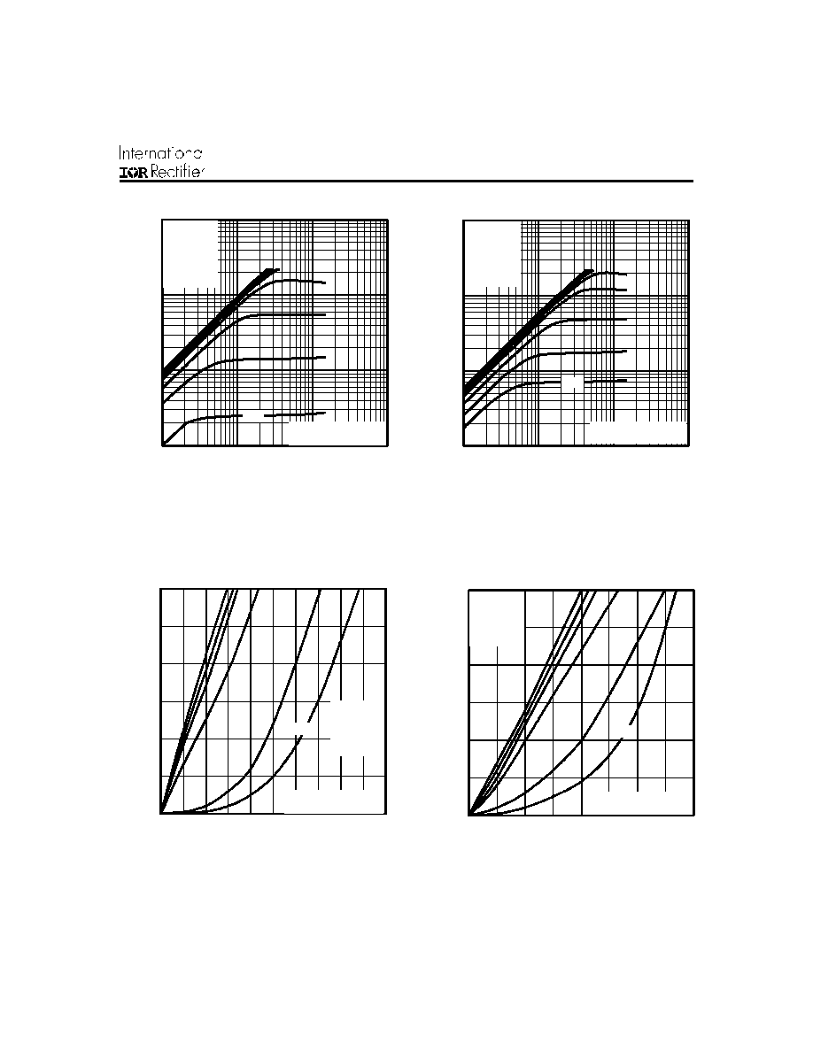
Fig 1. Typical Output Characteristics
Fig 2. Typical Output Characteristics
1
1 0
1 0 0
1 0 0 0
0.1
1
1 0
1 0 0
I
,
Dr
ai
n
-
t
o
-
S
ou
r
c
e Cur
r
e
n
t
(
A
)
D
V , D rain-to-S ou rce V o ltage (V )
D S
A
2 0µ s P U LS E W ID T H
T = 2 5°C
J
VGS
TOP 15V
12V
10V
8.0V
6.0V
4.0V
3.0V
BOTTOM 2.5V
2.5V
Fig 3. Typical Reverse Output Characteristics
Fig 4. Typical Reverse Output Characteristics
1
1 0
1 0 0
1 0 0 0
0.1
1
1 0
1 0 0
I , Drain-to-Source Current (A)
D
V , Drain-to-Source Voltage (V)
D S
A
VGS
TOP 15V
12V
10V
8.0V
6.0V
4.0V
3.0V
BOTTOM 2.5V
2 . 5 V
2 0 µ s P U L S E W I D T H
T = 150°C
J
0
1 0
2 0
3 0
0.0
0.2
0.4
0.6
0.8
V , D rain-to-S ource V olta ge (V)
D S
A
VG S
T O P 10V
8.0V
6.0V
4.0V
2.0V
B O T T O M 0.0V
0.0V
20µ s P U LS E W ID TH
T = 150°C
C
0
1 0
2 0
3 0
0.0
0.2
0.4
0.6
0.8
1.0
V , D rain-to-S ource V olta ge (V)
D S
20µ s P U LS E W ID TH
T = 25°C
C
A
VG S
T O P 10V
8.0V
6.0V
4.0V
2.0V
B O T T O M 0.0V
0.0V
I
S
, Source-to-Drain Current ( A )
I
S
, Source-to-Drain Current ( A )
IRL3103D2
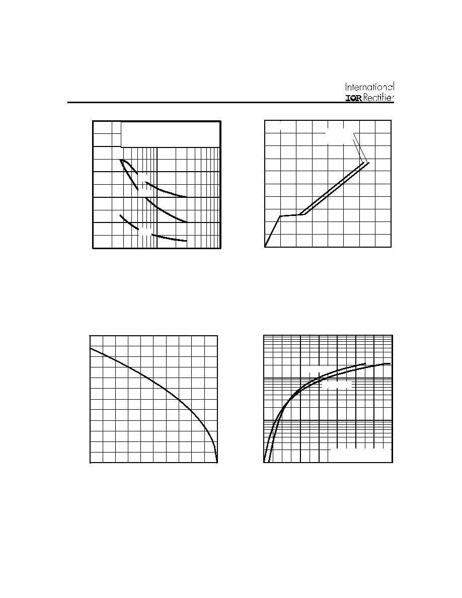
Fig 5. Typical Capacitance Vs.
Drain-to-Source Voltage
Fig 6. Typical Gate Charge Vs.
Gate-to-Source Voltage
Fig 7. Maximum Drain Current Vs.
Case Temperature
Fig 8. Typical Transfer Characteristics
25
50
75
100
125
150
0
10
20
30
40
50
60
T , Case Temperature ( C)
I , Drain Current (A)
°
C
D
1
1 0
1 0 0
1 0 0 0
2 . 0
3 . 0
4 . 0
5 . 0
6 . 0
7 . 0
8 . 0
9 . 0
T = 25°C
T = 150°C
J
J
G S
V , Gate-to-Source Voltage (V)
D
I , Drain-to-Source Current (A)
A
V = 15V
20µs PULSE WIDTH
D S
0
20
40
60
80
0
3
6
9
12
15
Q , Total Gate Charge (nC)
V , Gate-to-Source Voltage (V)
G
GS
I =
D
32A
V
= 15V
DS
V
= 24V
DS
0
1 0 0 0
2 0 0 0
3 0 0 0
4 0 0 0
5 0 0 0
1
1 0
1 0 0
D S
V , D rain-to-S o urce V oltage (V )
A
V = 0V , f = 1M H z
C = C + C , C SH O R T E D
C = C
C = C + C
G S
iss g s g d d s
rs s g d
os s d s g d
C
is s
C
oss
C
rs s
C, Capacitance ( pF )
IRL3103D2
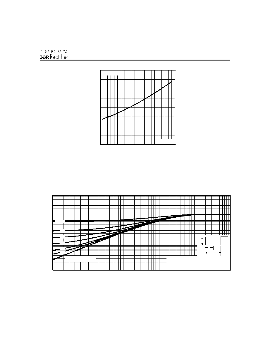
Fig 10. Maximum Effective Transient Thermal Impedance, Junction-to-Case
0 . 0 1
0 . 1
1
1 0
0 . 0 0 0 0 1
0 . 0 0 0 1
0 . 0 0 1
0 . 0 1
0 . 1
1
t , R e ctan gular P ulse D uration (se c)
1
th
J
C
D = 0.50
0 .0 1
0 .0 2
0.0 5
0 .1 0
0 .2 0
SING L E PU L SE
(T H ER M A L RE S PO N SE )
A
T
h
e
r
m
a
l
R
e
s
p
o
n
s
e
(
Z
)
P
t
2
1
t
D M
N o te s:
1 . D u ty fa c to r D = t / t
2 . P e a k T = P x Z + T
1
2
J
D M
th J C
C
Fig 9. Normalized On-Resistance
Vs. Temperature
-60 -40 -20
0
20
40
60
80 100 120 140 160
0.0
0.5
1.0
1.5
2.0
T , Junction Temperature ( C)
R , Drain-to-Source On Resistance
(Normalized)
J
DS(on)
°
V
=
I =
GS
D
10V
54A