Parameter
Max.
Units
I
D
@ T
C
= 25įC
Continuous Drain Current, V
GS
@ 10V
59
I
D
@ T
C
= 100įC
Continuous Drain Current, V
GS
@ 10V
41
A
I
DM
Pulsed Drain Current
230
P
D
@T
C
= 25įC
Power Dissipation
130
W
Linear Derating Factor
0.89
W/įC
V
GS
Gate-to-Source Voltage
Ī 10
V
E
AS
Single Pulse Avalanche Energy
320
mJ
I
AR
Avalanche Current
35
A
E
AR
Repetitive Avalanche Energy
13
mJ
dv/dt
Peak Diode Recovery dv/dt
2.2
V/ns
I
G
V
GS
Clamp Current
Ī 50
mA
V
ESD
Electrostatic Votage Rating
Ī 2.0
kV
T
J
Operating Junction and
-55 to + 175
įC
T
STG
Storage Temperature Range
Soldering Temperature, for 10 seconds
300 (1.6mm from case )
įC
Mounting torque, 6-32 or M3 srew
10 lbf∑in (1.1N∑m)
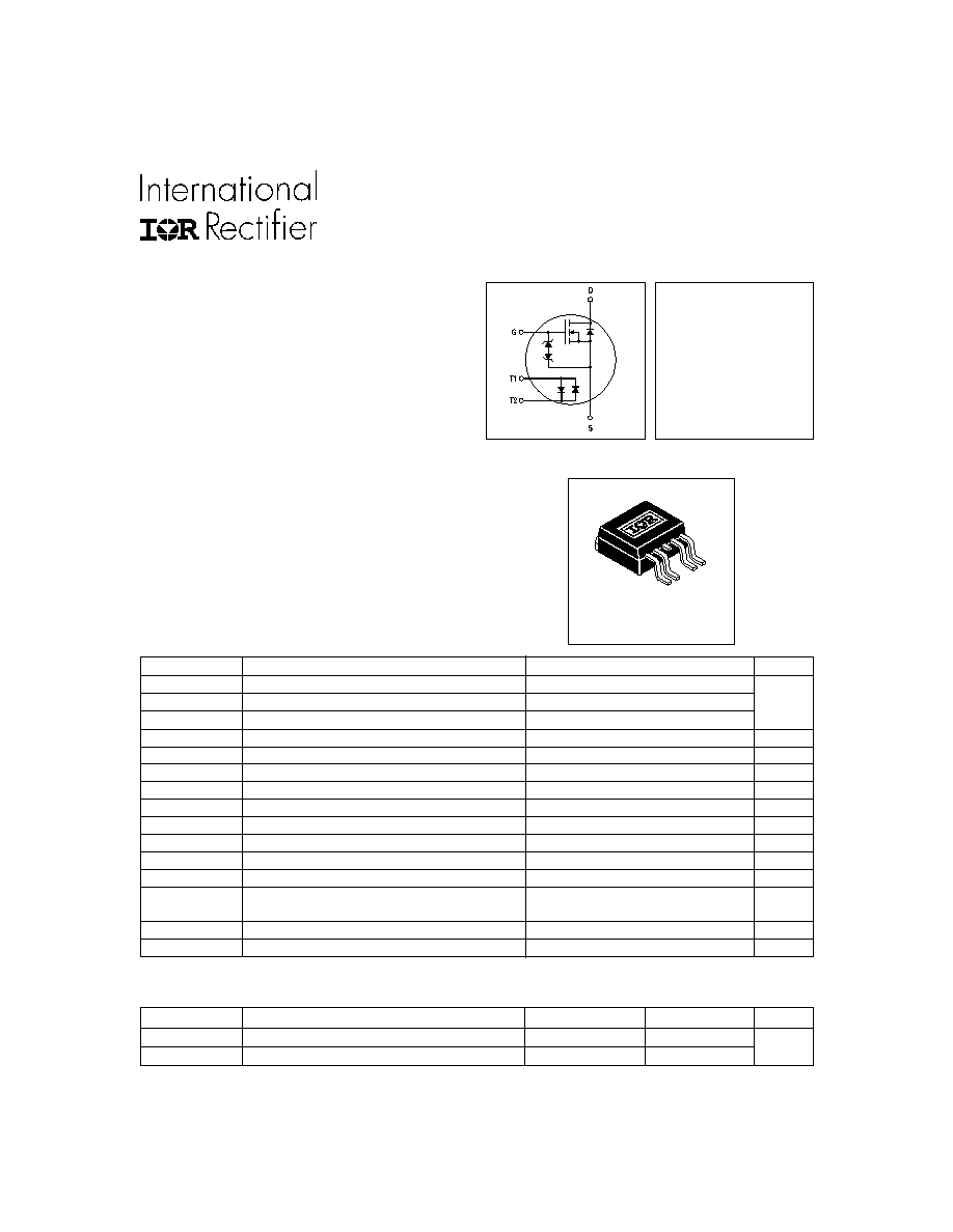
IRLBD59N04E
HEXFET
ģ
Power MOSFET
The IRLBD59N04E is a 40V, N-channel HEXFET
ģ
power MOSFET with gate protection provided by
integrated back to back zener diodes. Temperature
sensing is given by the change in forward voltage drop
of two antiparallel electrically isolated poly-silicon diodes.
The IRLBD59N04E provides cost effective temperature
sensing for system protection along with the quality and
ruggedness you expect from a HEXFET power MOSFET.
Absolute Maximum Ratings
Parameter
Typ.
Max.
Units
R
JC
Junction-to-Case
≠≠≠
1.12
įC/W
R
JA
Junction-to-Ambient ( PCB Mounted,steady-state)**
≠≠≠
40
Thermal Resistance
V
DSS
= 40V
R
DS(on)
= 0.018
I
D
= 59A
l
Integrated Temperature Sensing Diode
l
Ultra Low On-Resistance
l
Dynamic dv/dt Rating
l
175įC Operating Temperature
l
Fully Avalanche Rated
l
Zener Gate Protected
Description
4/11/00
PD -93910
www.irf.com
1
5 Lead-D
2
Pak
IRFLBD59N04E
2
www.irf.com
Parameter
Min. Typ. Max. Units
Conditions
V
(BR)DSS
Drain-to-Source Breakdown Voltage
40
≠≠≠
≠≠≠
V
V
GS
= 0V, I
D
= 250ĶA
V
(BR)DSS
/
T
J
Breakdown Voltage Temp. Coefficient
≠≠≠
0.036 ≠≠≠
V/įC
Reference to 25įC, I
D
= 1mA
≠≠≠
≠≠≠ 0.018
V
GS
= 10V, I
D
= 35A
≠≠≠
≠≠≠ 0.021
V
GS
= 5.0V, I
D
= 30A
V
GS(th)
Gate Threshold Voltage
1.0
≠≠≠
2.0
V
V
DS
= V
GS
, I
D
= 250ĶA
V
GS
Clamp Voltage
10
≠≠≠
20
V
I
GSS
= 20ĶA
g
fs
Forward Transconductance
29
≠≠≠
≠≠≠
S
V
DS
= 25V, I
D
= 35A
≠≠≠
≠≠≠
25
ĶA
V
DS
= 40V, V
GS
= 0V
≠≠≠
≠≠≠
250
V
DS
= 32V, V
GS
= 0V, T
J
= 150įC
Gate-to-Source Forward Leakage
≠≠≠
≠≠≠
1.0
V
GS
= 5.0V
Gate-to-Source Reverse Leakage
≠≠≠
≠≠≠
-1.0
V
GS
= -5.0V
Q
g
Total Gate Charge
≠≠≠
≠≠≠
53
I
D
= 35A
Q
gs
Gate-to-Source Charge
≠≠≠
≠≠≠
16
nC
V
DS
= 32V
Q
gd
Gate-to-Drain ("Miller") Charge
≠≠≠
≠≠≠
18
V
GS
= 5.0V, See Fig. 6 and 13
t
d(on)
Turn-On Delay Time
≠≠≠
7.9
≠≠≠
V
DD
= 20V
t
r
Rise Time
≠≠≠
110
≠≠≠
ns
I
D
= 35A
t
d(off)
Turn-Off Delay Time
≠≠≠
30
≠≠≠
R
G
= 5.1
,
t
f
Fall Time
≠≠≠
74
≠≠≠
V
GS
= 5.0V
,
See Fig.10
Between lead,
6mm (0.25in.)
from package
and center of die contact
C
iss
Input Capacitance
≠≠≠
2310 ≠≠≠
V
GS
= 0V
C
oss
Output Capacitance
≠≠≠
640
≠≠≠
V
DS
= 25V
C
rss
Reverse Transfer Capacitance
≠≠≠
130
≠≠≠
pF
= 1.0MHz, See Fig. 5
C
oss
Output Capacitance
≠≠≠
2250 ≠≠≠
V
GS
= 0V, V
DS
= 1.0V, = 1.0MHz
C
oss
Output Capacitance
≠≠≠
580
≠≠≠
V
GS
= 0V, V
DS
= 32V, = 1.0MHz
C
oss
eff.
Effective Output Capacitance
≠≠≠
530
≠≠≠
V
GS
= 0V, V
DS
= 0V to 32V
S
D
G
Parameter
Min. Typ. Max. Units
Conditions
I
S
Continuous Source Current
MOSFET symbol
(Body Diode)
≠≠≠
≠≠≠
showing the
I
SM
Pulsed Source Current
integral reverse
(Body Diode)
≠≠≠
≠≠≠
p-n junction diode.
V
SD
Diode Forward Voltage
≠≠≠
≠≠≠
1.3
V
T
J
= 25įC, I
S
= 35A, V
GS
= 0V
t
rr
Reverse Recovery Time
≠≠≠
54
81
ns
T
J
= 25įC, I
F
= 35A
Q
rr
Reverse RecoveryCharge
≠≠≠
90
130
nC
di/dt = 100A/Ķs
t
on
Forward Turn-On Time
Intrinsic turn-on time is negligible (turn-on is dominated by L
S
+L
D
)
Source-Drain Ratings and Characteristics
59
230
A
S
D
G
Electrical Characteristics @ T
J
= 25įC (unless otherwise specified)
R
DS(on)
Static Drain-to-Source On-Resistance
I
GSS
nH
L
S
Internal Source Inductance
≠≠≠
5.0
≠≠≠
L
D
Internal Drain Inductance
≠≠≠
2.0
≠≠≠
I
DSS
Drain-to-Source Leakage Current
Sense Diode Rating
Parameter
Min. Typ. Max. Units
Conditions
V
FM
Sense Diode Maximum Voltage Drop
675
≠≠≠
725
mV
I
F
= 250ĶA
V
F
/
T
J
Sense Diode Temperature Coefficient
-1.30 -1.40 -1.58 mV/įC I
F
= 250ĶA, See Fig.14
ĶA
IRLBD59N04E
www.irf.com
3
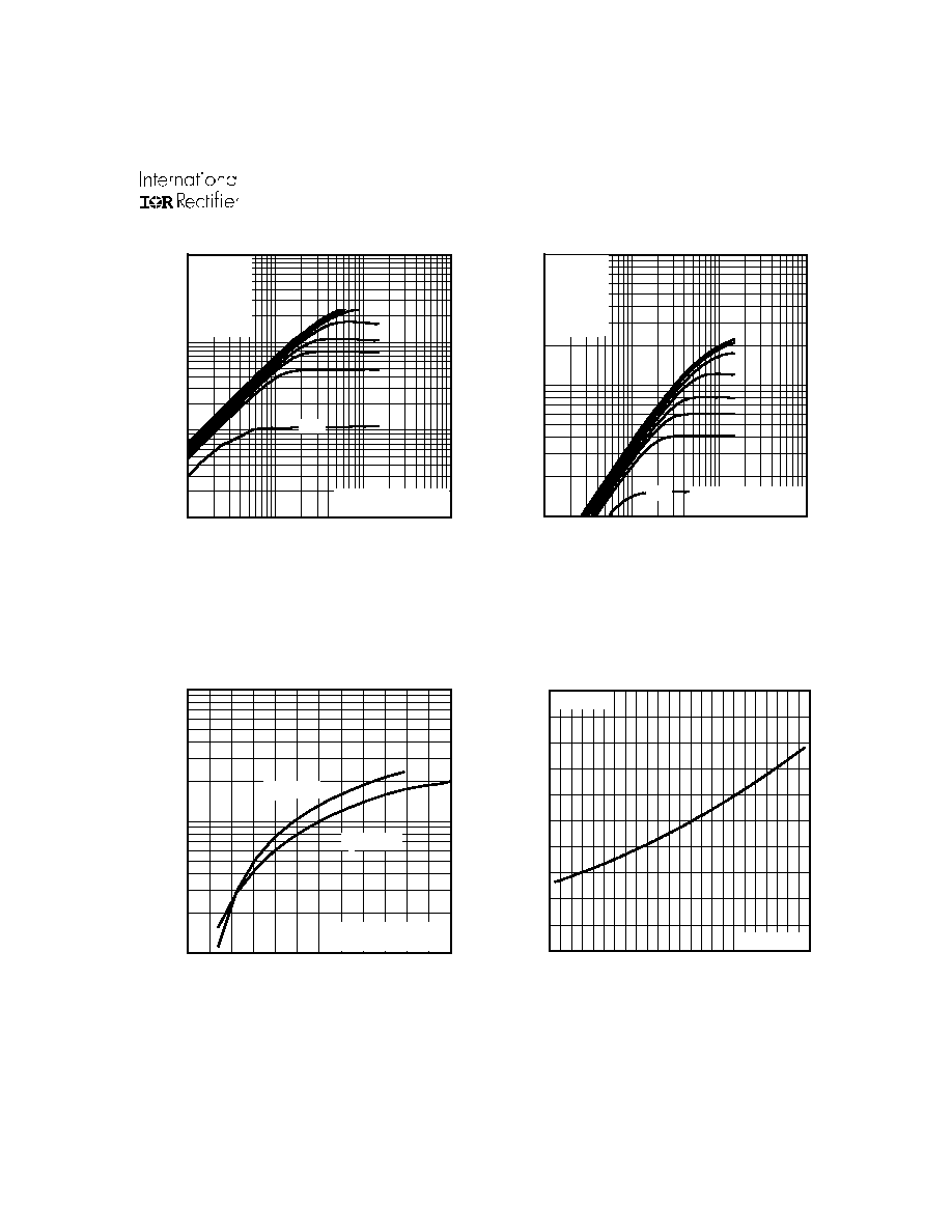
Fig 4. Normalized On-Resistance
Vs. Temperature
Fig 2. Typical Output Characteristics
Fig 1. Typical Output Characteristics
Fig 3. Typical Transfer Characteristics
1
10
100
1000
0.1
1
10
100
20Ķs PULSE WIDTH
T = 25 C
J
į
TOP
BOTTOM
VGS
15V
10V
7.0V
5.5V
4.5V
4.0V
3.5V
2.7V
V , Drain-to-Source Voltage (V)
I , Drain-to-Source Current (A)
DS
D
2.7V
10
100
1000
0.1
1
10
100
20Ķs PULSE WIDTH
T = 175 C
J
į
TOP
BOTTOM
VGS
15V
10V
7.0V
5.5V
4.5V
4.0V
3.5V
2.7V
V , Drain-to-Source Voltage (V)
I , Drain-to-Source Current (A)
DS
D
2.7V
10
100
1000
2.0
3.0
4.0
5.0
6.0
7.0
8.0
V = 15V
20Ķs PULSE WIDTH
DS
V , Gate-to-Source Voltage (V)
I , Drain-to-Source Current (A)
GS
D
T = 25 C
J
į
T = 175 C
J
į
-60 -40 -20
0
20 40 60 80 100 120 140 160 180
0.0
0.5
1.0
1.5
2.0
2.5
T , Junction Temperature ( C)
R , Drain-to-Source On Resistance
(Normalized)
J
DS(on)
į
V
=
I =
GS
D
10V
59A
IRFLBD59N04E
4
www.irf.com
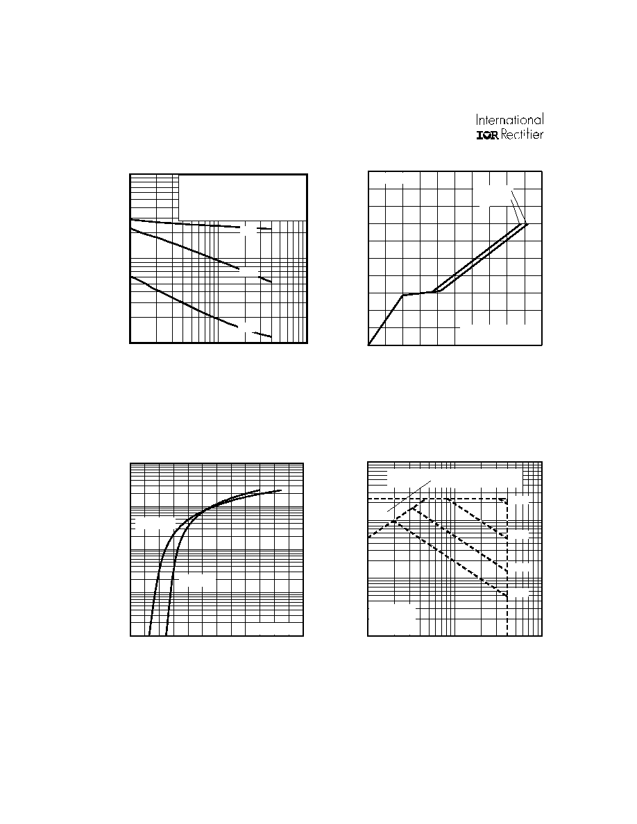
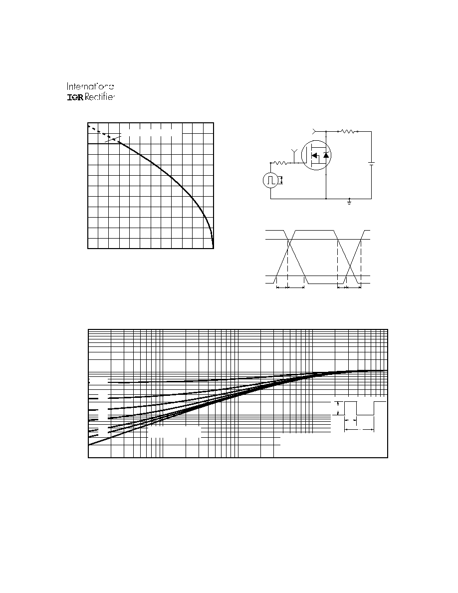
Fig 8. Maximum Safe Operating Area
Fig 6. Typical Gate Charge Vs.
Gate-to-Source Voltage
Fig 5. Typical Capacitance Vs.
Drain-to-Source Voltage
Fig 7. Typical Source-Drain Diode
Forward Voltage
0.1
1
10
100
1000
0.0
0.5
1.0
1.5
2.0
2.5
3.0
V ,Source-to-Drain Voltage (V)
I , Reverse Drain Current (A)
SD
SD
V = 0 V
GS
T = 25 C
J
į
T = 175 C
J
į
1
10
100
1000
1
10
100
OPERATION IN THIS AREA LIMITED
BY R
DS(on)
Single Pulse
T
T
= 175 C
= 25 C
į
į
J
C
V , Drain-to-Source Voltage (V)
I , Drain Current (A)
I , Drain Current (A)
DS
D
10us
100us
1ms
10ms
0
10
20
30
40
50
0
2
4
6
8
10
Q , Total Gate Charge (nC)
V , Gate-to-Source Voltage (V)
G
GS
FOR TEST CIRCUIT
SEE FIGURE
I =
D
13
35A
V
= 20V
DS
V
= 32V
DS
1
10
100
VDS, Drain-to-Source Voltage (V)
100
1000
10000
C, Capacitance(pF)
Coss
Crss
Ciss
VGS = 0V, f = 1 MHZ
Ciss = Cgs + Cgd, Cds SHORTED
Crss = Cgd
Coss = Cds + Cgd
IRLBD59N04E
www.irf.com
5
Fig 11. Maximum Effective Transient Thermal Impedance, Junction-to-Case
Fig 9. Maximum Drain Current Vs.
Case Temperature
0.01
0.1
1
10
0.00001
0.0001
0.001
0.01
0.1
Notes:
1. Duty factor D =
t / t
2. Peak T = P
x Z
+ T
1
2
J
DM
thJC
C
P
t
t
DM
1
2
t , Rectangular Pulse Duration (sec)
Thermal Response
(Z )
1
thJC
0.01
0.02
0.05
0.10
0.20
D = 0.50
SINGLE PULSE
(THERMAL RESPONSE)
V
DS
90%
10%
V
GS
t
d(on)
t
r
t
d(off)
t
f
V
DS
Pulse Width
1
Ķs
Duty Factor
0.1 %
R
D
V
GS
R
G
D.U.T.
V
GS
+
-
V
DD
25
50
75
100
125
150
175
0
10
20
30
40
50
60
T , Case Temperature
( C)
I , Drain Current (A)
į
C
D
LIMITED BY PACKAGE