Parameter
Max.
Units
I
D
@ Tc = 25∞C
Continuous Drain Current, V
GS
@ 5.0 V
1.5
I
D
@ Tc = 100∞C
Continuous Drain Current, V
GS
@ 5.0 V
0.93
I
DM
Pulsed Drain Current
12
P
D
@Tc = 25∞C
Power Dissipation
3.1
P
D
@T
A
= 25∞C
Power Dissipation (PCB Mount)**
2..0
W
Linear Derating Factor
0.025
Linear Derating Factor (PCB Mount)**
0.017
W/∞C
V
GS
Gate-to-Source Voltage
-/+10
V
E
AS
Single Pulse Avalanche Energy
50
mJ
I
AR
Avalanche Current
1.5
A
E
AR
Repetitive Avalanche Energy
0.31
mJ
dv/dt
Peak Diode Recovery dv/dt
5.5
V/ns
T
J,
T
STG
Junction and Storage Temperature Range
-55 to + 150
∞C
IRLL110
HEXFET
Æ
Power MOSFET
PD - 90869A
S
D
G
V
DSS
= 100V
R
DS(on)
= 0.54
I
D
= 1.5A
Third Generation HEXFETs from International Rectifier
provide the designer with the best combination of fast
switching, ruggedized device design, low on-resistance
and cost-effectiveness.
The SOT-223 package is designed for surface-mount using
vapor phase, infra red, or wave soldering techniques. Its
unique package design allows for easy automatic pick-and-
place as with other SOT or SOIC packages but has the
added advantage of improved thermal performance due to
an enlarged tab for heatsinking. Power dissipation of
grreater than 1.25W is possible in a typical surface mount
application.
1/27/99
Description
l
Surface Mount
l
Available in Tape & Reel
l
Dynamic dv/dt Rating
l
Repetitive Avalanche Rated
l
Logic-Level Gate Drive
l
RDS(on)Specified at VGS= 4V & 5V
l
Fast Switching
S O T -2 2 3
** When mounted on 1'' square PCB (FR-4 or G-10 Material).
For recommended footprint and soldering techniques refer to application note #AN-994.
Parameter
Typ.
Max.
Units
R
JC
Junction-to-PCB
≠≠≠
40
R
JA
Junction-to-Ambient. (PCB Mount)**
≠≠≠
60
Thermal Resistance
∞C/W
Absolute Maximum Ratings
A
www.irf.com
1
Soldewring Temperature, for 10 seconds
300 (1.6mm from case)
IRLL110
2
www.irf.com
Parameter
Min. Typ. Max. Units
Conditions
V
(BR)DSS
Drain-to-Source Breakdown Voltage
100
≠≠≠
≠≠≠
V
V
GS
= 0V, I
D
= 250µA
V
(BR)DSS
/
T
J
Breakdown Voltage Temp. Coefficient
≠≠≠
0.12
≠≠≠
V/∞C
Reference to 25∞C, I
D
= 1mA
≠≠≠
≠≠≠
0.54
V
GS
= 5.0V, I
D
= 0.90A
≠≠≠
≠≠≠
0.76
V
GS
= 4.0V, I
D
= 0.75A
V
GS(th)
Gate Threshold Voltage
1.0
≠≠≠
2.0
V
V
DS
= V
GS
, I
D
= 250µA
g
fs
Forward Transconductance
0.57
≠≠≠
≠≠≠
S
V
DS
= 25V, I
D
= 0.90 A
≠≠≠
≠≠≠
25
µA
V
DS
= 100V, V
GS
= 0V
≠≠≠
≠≠≠
250
V
DS
= 80V, V
GS
= 0V, T
J
= 125∞C
Gate-to-Source Forward Leakage
≠≠≠
≠≠≠
100
nA
V
GS
= 10V
Gate-to-Source Reverse Leakage
≠≠≠
≠≠≠
-100
V
GS
= -10V
Q
g
Total Gate Charge
≠≠≠
≠≠≠
6.1
I
D
= 5.6A
Q
gs
Gate-to-Source Charge
≠≠≠
≠≠≠
2.6
nC
V
DS
= 80V
Q
gd
Gate-to-Drain ("Miller") Charge
≠≠≠
≠≠≠
3.3
V
GS
= 5.0V, See Fig. 6 and 13
t
d(on)
Turn-On Delay Time
≠≠≠
9.3
≠≠≠
V
DD
= 50V
t
r
Rise Time
≠≠≠
47
≠≠≠
ns
I
D
= 5.6A
t
d(off)
Turn-Off Delay Time
≠≠≠
16
≠≠≠
R
G
= 12
t
f
Fall Time ≠≠≠ 18 ≠≠≠ R
D
= 8.4
,
nH
C
iss
Input Capacitance
≠≠≠
250
≠≠≠
V
GS
= 0V
C
oss
Output Capacitance
≠≠≠
80
≠≠≠
pF
V
DS
= 25V
C
rss
Reverse Transfer Capacitance
≠≠≠
15
≠≠≠
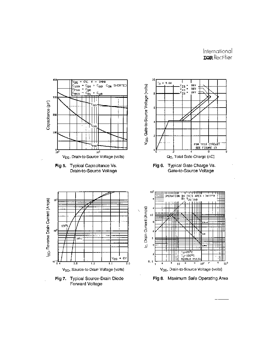
= 1.0MHz, See Fig. 5
Electrical Characteristics @ T
J
= 25∞C (unless otherwise specified)
I
GSS
R
DS(on)
Static Drain-to-Source On-Resistance
I
DSS
Drain-to-Source Leakage Current
Repetitive rating; pulse width limited by
max. junction temperature. ( See fig. 11 )
I
SD
5.6
A, di/dt
75A/µs, V
DD
V
(BR)DSS
,
T
J
150∞C
Notes:
V
DD
=25V, starting T
J
= 25∞C, L = 25 mH
R
G
= 25
, I
AS
= 1.5A. (See Figure 12)
Pulse width
300µs; duty cycle
2%.
Parameter
Min. Typ. Max. Units
Conditions
I
S
Continuous Source Current
MOSFET symbol
(Body Diode)
showing the
I
SM
Pulsed Source Current
integral reverse
(Body Diode)
p-n junction diode.
V
SD
Diode Forward Voltage
≠≠≠
≠≠≠
2.5
V
T
J
= 25∞C, I
S
= 1.5A, V
GS
= 0V
t
rr
Reverse Recovery Time
≠≠≠
110
130
ns
T
J
= 25∞C, I
F
= 5.6A
Q
rr
Reverse RecoveryCharge
≠≠≠
0.50
0.65
µC
di/dt = 100A/µs
t
on
Forward Turn-On Time
Intrinsic turn-on time is negligible (turn-on is dominated by L
S
+L
D
)
≠≠≠
≠≠≠
≠≠≠
≠≠≠
12
1.5
A
S
D
G
Between lead, 6mm(0.25in)
from package and center
of die contact.
L
S
Internal Source Inductance
Internal Drain Inductance
L
D
≠≠≠ 4.0 ≠≠≠
≠≠≠ 6.0 ≠≠≠
Source-Drain Ratings and Characteristics