 | ÐлекÑÑоннÑй компоненÑ: IRPT1058 | СкаÑаÑÑ:  PDF PDF  ZIP ZIP |
Äîêóìåíòàöèÿ è îïèñàíèÿ www.docs.chipfind.ru
page 1
PD 6.115
Integrated Power Stage for 0.75 hp Motor Drives
IRPT1058
PRELIMINARY
· 0.75 hp (0.56 kW) power output
Industrial rating at 150% overload for 1 minute
· 180 - 240V AC single-phase input, 50/60Hz
· Available as complete system or as sub-system
assemblies
Power Module
· Single-phase rectifier bridge
· 3-phase short circuit rated, ultrafast IGBT inverter
· Low inductance (current sense)
shunts in positive and negative DC rail
· NTC temperature sensor
· Pin-to-base plate isolation 2500V rms
· Easy-to-mount two-screw package
· Case temperature range -25
°
C to 125
°
C operational
Driver-
Plus Board
· DC bus capacitor filter with NTC inrush
current limiter
· IR2132 monolithic 3-phase HVIC driver
· On-board +15V and +5V power supply
· MOV surge suppression at input
· DC bus voltage and current feedback
· Protection for short-circuit, earth/ground fault and
overtemperature
· Terminal blocks for single-phase input and 3-phase
output connections
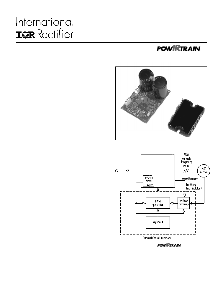
Figure 1. The IRPT1058C
within a motor
control system
IRPT1058C
180 - 240V
single-phase input

IRPT1058
page 2
The IRPT1058C
provides the complete
conversion function for a 0.75 hp (0.56 kW) variable frequency,
variable voltage, AC motor controller. The
combines a power module IRPT1058A with a Driver-Plus Board
IRPT1058D. Figure 1 shows the block diagram of the
within an AC motor control system.
The power module contains a single-phase input bridge
rectifier, 3-phase IGBT inverter, current sense shunts, and a
thermistor. It is designed for easy mounting to a heat sink. The
Driver-Plus Board contains DC link capacitors, capacitor soft
charge function using NTC thermistor, surge suppression MOV,
IGBT gate drivers, DC bus voltage and current feedback signals,
protection circuitry and local power supply. It is designed to mate
with a controller board through a single row header. Terminal
blocks are provided on the Driver-Plus Board for all end user line
input and motor output.
Output power is Pulse-Width Modulated (PWM) 3-phase,
variable frequency, variable voltage controlled by an externally
generated user-provided PWM controller for inverter IGBT
switching. The power supply offers the user non-isolated 5V and
15V to power the micro-controller.
The IRPT1058C offers several benefits to the drive
manufacturer listed below:
·
It greatly simplifies component selection, design of layout,
interconnection, gate drive, local power supply, thermal
sensing, current sensing and protection.
·
Gate drive and protection circuits are designed to closely
match the operating characteristics of the power
semiconductors. This allows power losses to be minimized and
power rating to be maximized to a greater extent than is
possible by designing with individual components.
·
It reduces the effort of calculating and evaluating power
semiconductor losses and junction temperature.
·
It reduces the manufacturer's part inventory and simplifies
assembly.
[
specifications and ratings are given for system
input and output voltage and current, power losses and heat sink
requirements over a range of operating conditions.
system ratings are verified by IR in final testing.]
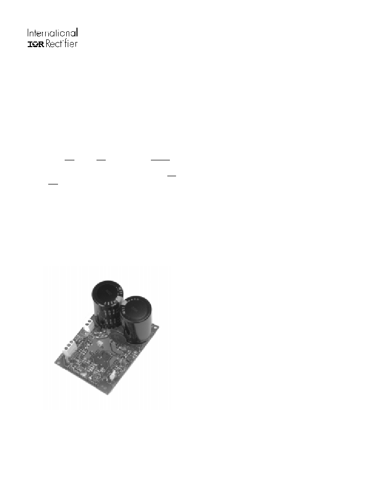
The IRPT1058A Power Module
The IRPT1059A Power Module, shown in figure 2, is a chip
and wire epoxy encapsulated module. It houses input rectifiers
output inverter, current sense shunts and NTC thermistor. The
single-phase input bridge rectifiers are rated at 800V. The
inverter section employs 600V, short circuit rated, ultrafast
IGBTs
and ultrafast freewheeling diodes. Current sensing is
achieved through 75m
low inductance shunts
provided in the
positive and negative DC bus rail. The NTC thermistor
provides temperature sensing capability. The lead spacing on the
power module meets UL840 pollution level 3 requirements.
The power circuit and layout within the module are carefully
designed to minimize inductance in the power path, to reduce
noise during inverter operation and to improve the inverter
efficiency. The Driver-Plus Board required to run the inverter
can be soldered to the power module pins, thus minimizing
assembly and alignment. The power module is designed to be
mounted to a heat sink with two screw mount positions, in order
to insure good thermal contact between the module substrate and
the heat sink.
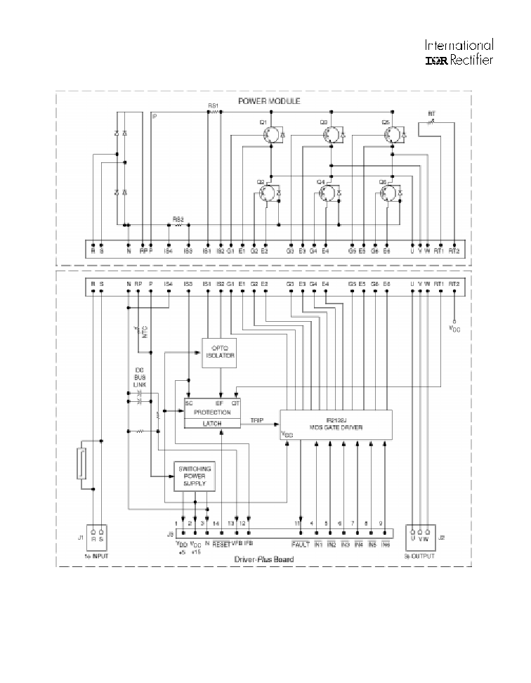
System Description
Figure 2. IRPT1058C Power Module
IRPT1058
page 3
Figure 3. IRPT1058D Driver-
Plus Board
The protection circuitry receives current signals from shunts
in positive and negative DC bus rail for earth/ground fault and
short-circuit
conditions. Any earth-fault signal is fed through an
opto-isolator to the protection circuitry. Current signal from
negative DC bus rail is provided on the J3 connector as current
feedback
, IFB (0.075V/A). If filtering of this signal is required,
it should be done by adding a high-impedance buffer stage
between signal and filter. DC bus voltage is scaled down to
provided a voltage signal on the J3 connector as voltage
feedback
, VFB (0.023 x Bus voltage). Thermal sense signal for
over-temperature
protection is obtained from a thermistor
housed inside the power module. The thermistor activates the
latch if the temperature of the power module's IMS substrate
exceeds a set level.
The system is designed for 150% overload for one minute
while operating with the specified heat sink. The external
microcontroller should shut off PWM signals if the overload
condition persists for more than one minute.
The switching power supply employs the IR2152S self-
oscillating driver chip in a buck regulator topology to deliver
nominal 15V and 5V DC outputs, referenced to the negative DC
bus (N). The power supply feeds the gate drive and protection
circuits. The 15V and 5V outputs are available on the control
interface connector's (J3) VCC and VDD pins for external
microprocessor and control logic supply.
The IRPT1058D Driver-
Plus Board
The IRPT1058D Driver-Plus board, shown in figure 3, houses
surge suppression MOV on input, a switching power supply, a DC
bus filter capacitor with NTC inrush current limiter, an IR2132J
monolithic 3-phase driver IC, and protection and sensing circuitry.
The inverter gate drive circuit, implemented with an IR2132J
monolithic 3-phase HVIC driver, delivers on/off gate drive
signals to the IGBTs' gates, corresponding with input PWM
control signals IN1 through IN6. After power-up, RESET pin on
the J3 connector must be held low (with open collector
configuration) for at least 2
µ
sec while all PWM signals, IN1
through IN6 are held high (off condition). A latch in the
protection circuitry is set high during a fault condition to trip the
IR2132J's internal latch and shut down all PWM output gate
drive signals and cause the FAULT output pin on IR2132J to set
low and light the LED. The Fault diagnostic is an active low,
open drain output with a pull-up resistor. This signal is provided
on the J3 connector for fault feedback to external control logic.
IRPT1058
page 4
Figure 4. IRPT1058C Basic Architecture

IRPT1058
page 5
PARAMETERS
VALUES
CONDITIONS
Input Power
Voltage
220V, -15%, +10%, single-phase
Frequency
50/60 Hz
Input current
10.5A rms @ nominal output
T
A
= 40
°
C, R
thSA
= 1.69
°
C/W
150A peak
Initial bus capacitor charging
Output Power
Voltage
0 - 230V
defined by external PWM control
Nominal Motor hp (kW)
0.75 hp (0.56 kW) nominal full load power V
in
= 230V, f
pwm
= 4 kHz, f
o
= 60 Hz
150% overload for 1 minute
T
A
= 40
°
C, R
thSA
= 1.69
°
C/W
Nominal motor current
3.3A nominal full load current
Z
thSA
limits DT
c
to 10
°
C during overload
4.95A 150% overload for 1 minute
Control Inputs
PWM input signals IN1...IN6
5V maximum, active low
CMOS, LSTTL compatible, open collector
Pulse deadtime
0.8
µ
sec typ. deadtime set by IR2132J
max. deadtime set by external controller
Minimum input pulse width
1
µ
sec
RESET
open collector, active low
pin 14 of control interface connector
pull down for
2
µ
sec to release latch
Protection
Output current trip level
18A,
±
10%
T
C
= 25
°
C
Earth/gnd fault current trip level
22A,
±
10%
T
C
= 25
°
C
Overtemperature trip level
100
°
C,
±
5%
Case temperature
Maximum DC link voltage
400V
user to ensure rating not exceeded for >30 sec.
Short circuit shutdown time
2.5
µ
sec typical
output terminals shorted
Feedback Signals
Current feedback (IFB)
0.075V/A
DC bus voltage feedback (VFB)
0.023 typical V/V
BUS
Fault feedback (Fault)
5V, active low
On Board Power Supply
V
CC
15V,
±
10%
V
DD
5V,
±
5%
I
CC
+ I
DD
60 mA
max. limit specified is available on control
interface connector J3 for external use
Module
Isolation voltage
2500V rms
pin to base plate isolation, 60 Hz, 1 minute
Operating case temperature
-25
°
C to 125
°
C
95%RH max. (non-condensing)
Mounting torque
1 Nm
M4 screw type
System Environment
Ambient operating temp. range
0 to 40
°
C
95%RH max. (non-condensing)
Storage temperature range
-25 to 60
°
C
Specifications