 | –≠–ª–µ–∫—Ç—Ä–æ–Ω–Ω—ã–π –∫–æ–º–ø–æ–Ω–µ–Ω—Ç: IRPT4052 | –°–∫–∞—á–∞—Ç—å:  PDF PDF  ZIP ZIP |

page 1
IRPT 4052
Revised 3/25/97
PD 6.096
TM
Integrated Power Stage for 7.5 hp Motor Drives
IRPT4052
PRELIMINARY
∑ 7.5 hp (5.5kW) power output
Industrial rating at 150% overload for 1 minute
∑ 380 - 480V AC input, 50/60Hz
∑ Available as complete system or sub-system assemblies
Power Assembly
∑ 3-phase rectifier bridge
∑ 3-phase short circuit rated, ultrafast IGBT inverter
∑ HEXFREDTM UltraFastTM soft recovery free-wheeling
diode
∑ NTC temperature sensor
∑ Pin-to-base plate isolation 2500V rms
∑ Easy-to-mount package
∑ Case temperature range -25 C to 125 C operational
Driver-
Plus Board
∑ Capacitor filter with precharge current limit
∑ Isolated gate drive circuits
∑ On-board local power supply for gate driver and
capacitor precharge control
∑ MOV surge suppression at input
∑ Isolated inverter current feedback
∑ Short circuit, earth/ground fault, over-temperature
protection
∑ Input and output terminals;
optional external brake
∑ Control interface connector
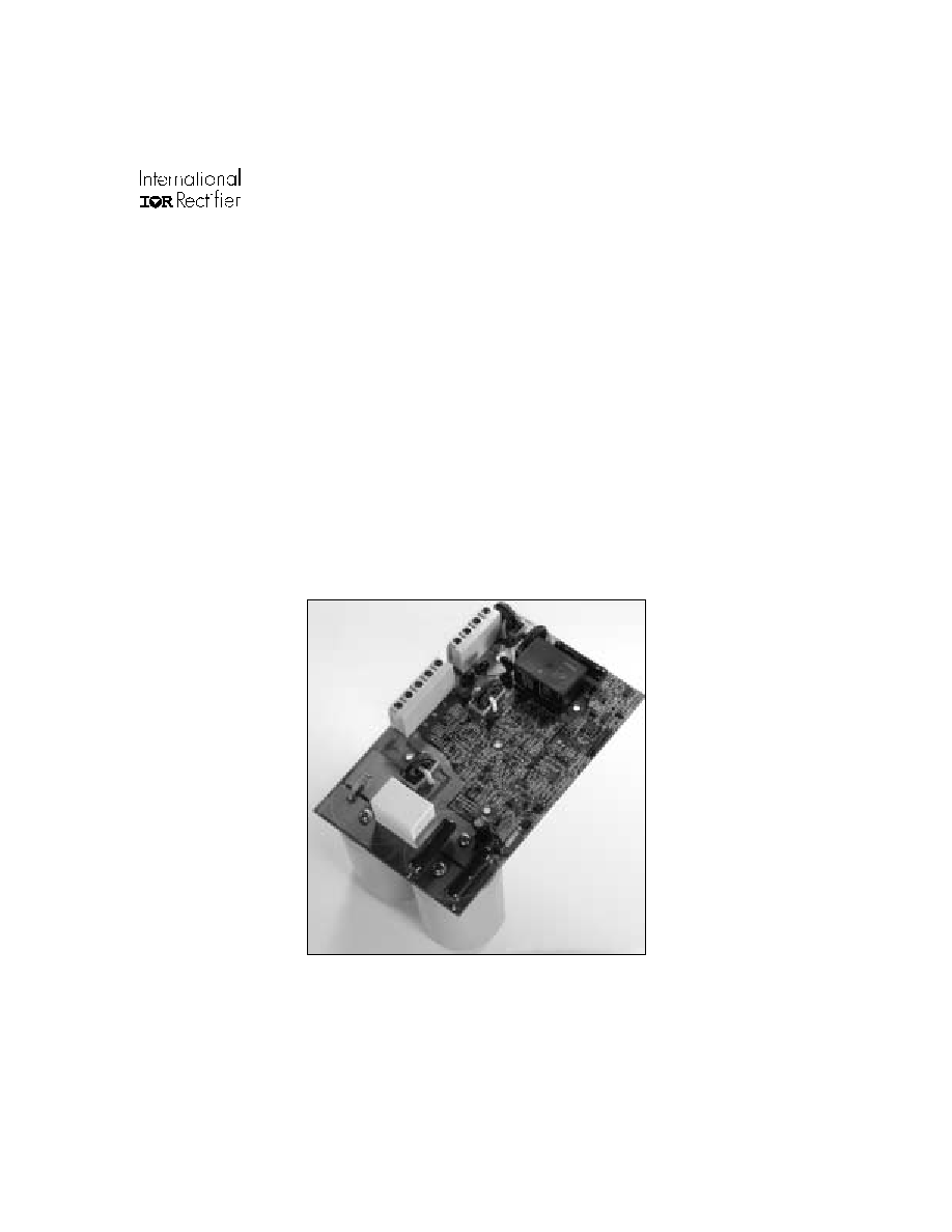
Figure 1. The IRPT4052C
within a motor
control system

page 2
IRPT 4052
System Description
The IRPT4052C
provides the complete
power conversion function for a 7.5hp (5.5kW) variable voltage,
variable frequency, AC motor controller. The
combines a power assembly IRPT4052A with a Driver-Plus
Board IRPT4052D. Figure 1 shows the block diagram of the
within an AC motor control system.
The power assembly contains a 3-phase input bridge rectifier,
3-phase IGBT inverter and a thermistor mounted on an Insulated
Metal Substrate (IMS) power board. It is designed for easy
mounting to a heat sink.
The Driver-Plus Board contains DC link capacitors, capacitor
pre-charge function, isolated IGBT gate drive circuits, shutdown
protection, isolated trip and current feedback signals, and local
power supply. It interfaces to the power assembly via soldered
connector pins. Terminal blocks are provided on the Driver-Plus
Board for all end-user external connections to the
.
Output power is Pulse-Width Modulated (PWM), 3-phase,
variable-frequency, variable voltage controlled by externally
generated user provided PWM controller for inverter IGBT
switching. The PWM input signals and feedback signals are opti-
cally isolated from the power circuit.
The IRPT4052C offers several benefits to the drive manufac-
turer as listed below:
∑ It eliminates component selection, design layout, intercon-
nection, gate drive, local power supply, thermal sensing,
current sensing, and protection.
∑ It provides committed power semiconductor losses and
junction temperatures.
∑ Gate drive and protection circuits are designed to closely
match the operating characteristics of the power semicon-
ductors. This allows power losses to be minimized and
power rating to be maximized to a greater extent than is
possible by designing with individual components.
∑ Optimized layout for performance and efficiency is pro-
vided.
∑ Low inductance system reduces noise and snubber require-
ments.
[
specifications and ratings are given for
system input and output voltage and current, power losses
and heat sink requirements over a range of operating con-
ditions.
system ratings are verified by IR
in final testing.]
Power Assembly
The IRPT4052A power assembly consists of input rectifiers,
NTC thermistor, output inverter and connectors mounted on an
Insulated Metal Substrate (IMS) substrate. The input side em-
ploys surface mount 1600V rated SMD-220 rectifier diodes and
the inverter section employs surface mount SMD-10, 1200V
IGBT Co-pack switches. The NTC thermistor mounted near the
inverter provides temperature sensing capability. The lead spac-
ing on the power assembly meets UL840 pollution level 2
requirements.
The power circuit and layout are carefully designed to mini-
mize inductance in the power path, to reduce noise during
inverter operation and to improve the inverter efficiency. The
power level interfaces to the Driver-Plus Board through solder
pins, minimizing assembly and alignment. The power assembly
is designed to be mounted to a heat sink with five screw mount
positions, one in each corner and a fifth near the center, in order
to insure good thermal contact between the IMS and the heat
sink.
The IRPT4052D Driver-
Plus Board
The Driver-Plus Board, shown in figure 3, is the interface be-
tween the controller and the power stage. It contains the IGBT
gate drivers, sensing and protection circuitry, feedback and local
power supply. It also houses the DC link capacitors, relay and
relay control circuit used for implementing the capacitor pre-
charge function. Figure 4 provides detailed functional block
diagrams of the IRPT4052D.
The gate drive circuits deliver on/off gate drive signals to the
IGBTs' gates, corresponding with input PWM control signals
IN1 through IN6. The PWM gate normally allows the input
PWM control signal to pass to the input opto-isolators of the
gate drive circuits. The conduction periods of the inverter
switches essentially mimic those demanded by the PWM input
signals.
Figure 2. IRPT4052A Power Assembly
page 3
IRPT 4052
During power-up and power-down, or in the event of
overcurrent (OI) or overtemperture (OT), the latch inhibits the
PWM gate, deactivating the gate drive circuits and shutting off
the inverter.
The relay control circuit delivers an on/off signal via an
opto-isolator to the relay driver which controls the relay (K1).
The relay contact is open during power-up, inserting the resistor
R in series with the DC bus capcitor and limiting the capacitor
charging current. In normal operation, the relay contact is closed.
If the AC line voltage falls below 300V or if one input phase is
lost, or if the DC line voltage falls to less than 82% of the peak
line voltage, the relay contact opens.
The UV circuit senses the voltage of the local power supply,
and sends a signal via an opto-isolator to the latch in the event of
undervoltage. The UV circuit normally activates the latch only
during power-up and power-down, preventing the IGBTs from
being turned on when the local power supply voltage is too low
for proper IGBT switching.
The current signal processing circuit receives inputs from
current transformers connected in series with the input lines and
the DC bus capacitor. The output of the current signal processing
circuit, IFB, is essentially an isolated replica of the inverter input
current. An isolated current feedback signal, I
FB
, is provided as
an output of the IRPT4052A. If the inverter current exceeds the
trip level of 45A, I
FB
also activates the latch.
The thermistor activates the latch if the temperature of the
IMS substrate exceeds a set level. The 15V isolated power sup-
ply used to power the IRPT4052 should be the same as the one
for the PWM generation, otherwise the protection functions will
be disabled.
The switching power supply delivers a nominal 18V DC out-
put, referenced to the negative DC bus, N. This feeds the gate
drive, relay control and under voltage (UV) circuits, which are
optically isolated from the control input section, and therefore
require their own local power source.
Figure 3. IRPT4052D Driver-
Plus Board

page 4
IRPT 4052
Figure 4. IRPT4052C Basic Architecture
INPUT RECTIFIER
P
Q2
Q4
Q6
Q1
Q3
Q5
RT2
RT1
W
V
U
E6
G6
E5
G5
E4
G4
E3
G3
E2
G2
E1
G1
N
P
RP
T
S
R
RELAY
CONTACT
(K1)
SWITCHING
POWER
SUPPLY
CURRENT
SIGNAL
PROCESSING
12 13 14
18
4
5
6
POWER TB
CN6B
OUTPUT RECTIFIER
IMS POWER ASSEMBLY
RT2
RT1
W
V
U
E6
G6
E5
G5
E4
G4
E3
G3
E2
G2
E1
G1
N
P
RP
T
S
R
THERMISTOR
DC LINK CAPS
PRE-
CHARGER
RELAY DRIVER
AND
RELAY COIL
(K1)
LATCH
OI, OT, UV
PWM GATE
OPTO ISOLATION
RELAY CONTROL
AND UV
CAP SENSE
CT
+18
GATE DRIVER CIRCUITS
OPTO ISOLATION
POWER TB
CN6B
SIGNAL
TB
1
2
3
16
7
8
9
19 20 15
GND
R S T
P U V W
N
IN6
IN5
IN4
IN3
CN5
IN2
IN1
UV
OT
OI
RESET
KIFB
SFT
CHG
BUS
RIPPLE
IFB
≠15
COM
+15
Driver-
Plus Board

page 5
IRPT 4052
PARAMETERS
VALUES
CONDITIONS
Input Power
Voltage
380V, -15%, 480V +10%, 3-phase
Frequency
50 - 60Hz
Input current
20A rms
T
A
= 40∞C, R
thSA
= 0.148∞C/W
300 A peak
10ms half-cycle, non-repetitive surge
Output Power
Voltage
0 - 480V rms
defined by external PWM control
Nominal motor hp (kW)
7.5hp (5.5 kW) nominal full load power
V
in
= 440VAC
150% overload for 1 minute
PWM frequency = 4kHz, f
∞
=60Hz,
Nominal motor current
12.5A rms nominal full load current
T
A
= 40∞C, R
thSA
= 0.148∞C/W
18.75A rms 150% overload for 1 minute
DC Link
DC link voltage
850V maximum
Control Inputs
Control power
15V ±5%, 200mA positive supply
15V ±5%, 10mA negative supply
PWM input signals IN1 - IN6
15V, 10mA, ±10% (max rise/fall time 150nsec)
input signals uninhibited internally
Input resistance IN1 - IN6
720 ohms ±5%
input signals inhibited internally
Pulse deadtime
2.5
µsec, minimum
Minimum input pulse duration
1.0
µsec
Maximum pulse duration for
20ms
each upper IGBT
RESET
15V active high, CMOS input
(min duration 1
µsec)
SFT CHG
2 mA pull-down to energize relay
(overrides internal control)
Protection
Output current trip level
45A peak, ±10%
Overtemperature trip level
100∞C, ±5%
Ground current trip level
40A peak, ±10%
Short circuit shutdown time
1.5
µsec typical
output terminals shorted
Feedback Signals
Current feedback signal, IFB
100mV/A ±10%
max. DC offset 200mV
Overcurrent trip signal, OI
active high, 15V CMOS
Overtemp trip signal, OT
active high, 15V CMOS
15V high 4.7k pull-up, <0.5V low at 1.0mA;
BUS RIPPLE
high-to-low transition at V
bus
=82% peak
of line voltage
UV
15V high, 10k pull-up, during UV
<0.5 low at 1mA with no UV
Relay coil feedback, K1FB
15V high when relay coil energized; low when
relay coil de-energized
Capacitor Precharge
DC bus capacitor precharge time
400msecs max
measured from input line closure;
line voltage > 300V
Module
Isolation voltage
2500V rms
pin-to-baseplate, 60Hz, 1 min.
Operating case temperature
-25∞C to 125∞C
95% RH max. (non-condensing)
Mounting torque
5 Nm
M5 screw type
System Environment
Ambient operating temp. range
0 to 40∞C
95% RH max. (non-condensing)
Storage temp.range
-25∞C to 60∞C
Specifications