 | –≠–ª–µ–∫—Ç—Ä–æ–Ω–Ω—ã–π –∫–æ–º–ø–æ–Ω–µ–Ω—Ç: Si4410DY | –°–∫–∞—á–∞—Ç—å:  PDF PDF  ZIP ZIP |

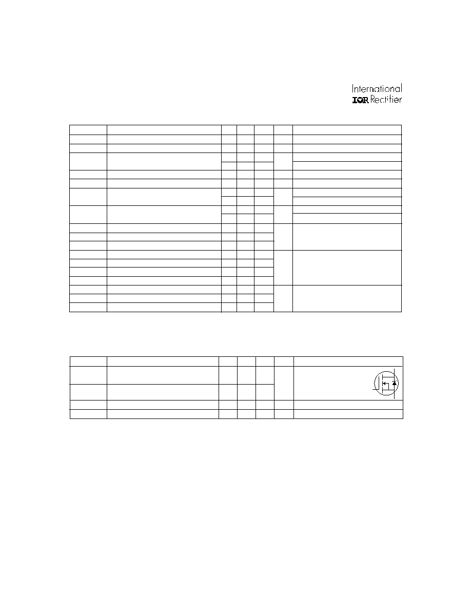
Parameter
Max.
Units
V
DS
Drain- Source Voltage
30
V
I
D
@ T
A
= 25∞C
Continuous Drain Current, V
GS
@ 10V
±10
I
D
@ T
A
= 70∞C
Continuous Drain Current, V
GS
@ 10V
±8.0
A
I
DM
Pulsed Drain Current
±50
P
D
@T
A
= 25∞C
Power Dissipation
2.5
P
D
@T
A
= 70∞C
Power Dissipation
1.6
Linear Derating Factor
0.02
W/∞C
dv/dt
Peak Diode Recovery dv/dt
5.0
V/ns
E
AS
Single Pulse Avalanche Energy
400
mJ
V
GS
Gate-to-Source Voltage
± 20
V
T
J,
T
STG
Junction and Storage Temperature Range
-55 to + 150
∞C
l
N-Channel MOSFET
l
Low On-Resistance
l
Low Gate Charge
l
Surface Mount
l
Logic Level Drive
11/22/99
Si4410DY
HEXFET
Æ
Power MOSFET
Parameter
Max.
Units
R
JA
Maximum Junction-to-Ambient
50
∞C/W
Thermal Resistance
This N-channel HEXFET
Æ
Power MOSFET is produced
using International Rectifier's advanced HEXFET power
MOSFET technology. The low on-resistance and low gate
charge inherent to this technology make this device ideal
for low voltage or battery driven power conversion
applications
The SO-8 package with copper leadframe offers enhanced
thermal characteristics that allow power dissipation of
greater that 800mW in typical board mount applications.
V
DSS
= 30V
R
DS(on)
= 0.0135
Description
T o p V ie w
8
1
2
3
4
5
6
7
D
D
D
D
G
S
A
S
S
A
Absolute Maximum Ratings
W
www.irf.com
1
PD - 91853C
SO-8
Si4410DY
2
www.irf.com
Parameter
Min. Typ. Max. Units
Conditions
I
S
Continuous Source Current
MOSFET symbol
(Diode Conduction)
showing the
I
SM
Pulsed Source Current
integral reverse
(Body Diode)
p-n junction diode.
V
SD
Diode Forward Voltage
≠≠≠
0.7
1.1
V
T
J
= 25∞C, I
S
= 2.3A, V
GS
= 0V
t
rr
Reverse Recovery Time
≠≠≠
50
80
ns
T
J
= 25∞C, I
F
= 2.3A
Repetitive rating; pulse width limited by
max. junction temperature.
Notes:
Pulse width
300µs; duty cycle
2%.
Source-Drain Ratings and Characteristics
≠≠≠
≠≠≠
≠≠≠
≠≠≠
50
2.3
A
S
D
G
When mounted on FR4 Board, t
10 sec
Parameter
Min. Typ. Max. Units
Conditions
V
(BR)DSS
Drain-to-Source Breakdown Voltage
30
≠≠≠
≠≠≠
V
V
GS
= 0V, I
D
= 250µA
V
(BR)DSS
/
T
J
Breakdown Voltage Temp. Coefficient
≠≠≠ 0.029 ≠≠≠
V/∞C
Reference to 25∞C, I
D
= 1mA
≠≠≠ 0.010 0.0135
V
GS
= 10V, I
D
= 10A
≠≠≠ 0.015 0.020
V
GS
= 4.5V, I
D
= 5.0A
V
GS(th)
Gate Threshold Voltage
1.0
≠≠≠
≠≠≠
V
V
DS
= V
GS
, I
D
= 250µA
g
fs
Forward Transconductance
≠≠≠
35
≠≠≠
S
V
DS
= 15V, I
D
= 10A
≠≠≠
≠≠≠
1.0
V
DS
= 30V, V
GS
= 0V
≠≠≠
≠≠≠
25
V
DS
= 30V, V
GS
= 0V, T
J
= 55∞C
Gate-to-Source Forward Leakage
≠≠≠
≠≠≠
-100
V
GS
= -20V
Gate-to-Source Reverse Leakage
≠≠≠
≠≠≠
100
V
GS
= 20V
Q
g
Total Gate Charge
≠≠≠
30
45
I
D
= 10A
Q
gs
Gate-to-Source Charge
≠≠≠
5.4
≠≠≠
nC
V
DS
= 15V
Q
gd
Gate-to-Drain ("Miller") Charge
≠≠≠
6.5
≠≠≠
V
GS
= 10V, See Fig. 10
t
d(on)
Turn-On Delay Time
≠≠≠
11
≠≠≠
V
DD
= 25V
t
r
Rise Time
≠≠≠
7.7
≠≠≠
I
D
= 1.0A
t
d(off)
Turn-Off Delay Time
≠≠≠
38
≠≠≠
R
G
= 6.0
t
f
Fall Time
≠≠≠
44
≠≠≠
R
D
= 25
,
C
iss
Input Capacitance
≠≠≠ 1585 ≠≠≠
V
GS
= 0V
C
oss
Output Capacitance
≠≠≠
739
≠≠≠
pF
V
DS
= 15V
C
rss
Reverse Transfer Capacitance
≠≠≠
106
≠≠≠
= 1.0MHz, See Fig. 9
Electrical Characteristics @ T
J
= 25∞C (unless otherwise specified)
I
GSS
µA
R
DS(on)
Static Drain-to-Source On-Resistance
I
DSS
Drain-to-Source Leakage Current
nA
ns
Starting T
J
= 25∞C, L = 8.0mH
R
G
= 25
, I
AS
= 10A. (See Figure 15)
I
SD
2.3A, di/dt
130A/µs, V
DD
V
(BR)DSS
,
T
J
150∞C

Si4410DY
www.irf.com
3
Fig 4. Normalized On-Resistance
Vs. Temperature
Fig 2. Typical Output Characteristics
Fig 1. Typical Output Characteristics
Fig 3. Typical Transfer Characteristics
10
100
1000
0.1
1
10
100
20µs PULSE WIDTH
T = 25 C
J
∞
TOP
BOTTOM
VGS
15V
10V
8.0V
7.0V
6.0V
5.5V
5.0V
4.5V
V , Drain-to-Source Voltage (V)
I , Drain-to-Source Current (A)
DS
D
4.5V
10
100
1000
0.1
1
10
100
20µs PULSE WIDTH
T = 150 C
J
∞
TOP
BOTTOM
VGS
15V
10V
8.0V
7.0V
6.0V
5.5V
5.0V
4.5V
V , Drain-to-Source Voltage (V)
I , Drain-to-Source Current (A)
DS
D
4.5V
-60 -40 -20
0
20
40
60
80 100 120 140 160
0.0
0.5
1.0
1.5
2.0
T , Junction Temperature ( C)
R , Drain-to-Source On Resistance
(Normalized)
J
DS(on)
∞
V
=
I =
GS
D
10V
11A
1 0
1 0 0
1 0 0 0
4
8
1 2
1 6
T = 2 5 ∞ C
J
G S
V , G a te-to-S ou rce V olta ge (V )
D
I
,
D
r
a
i
n
-
t
o
-
S
o
u
rc
e
C
u
rre
n
t
(A
)
A
V = 2 5 V
2 0 µ s P U L S E W ID T H
D S
T = 1 5 0 ∞ C
T = -5 5 ∞ C
J
J
10A

Si4410DY
4
www.irf.com
Fig 8. Maximum Safe Operating Area
Fig 6. Typical Gate Charge Vs.
Gate-to-Source Voltage
Fig 5. Typical Capacitance Vs.
Drain-to-Source Voltage
Fig 7. Typical Source-Drain Diode
Forward Voltage
0.1
1
10
100
0.4
0.5
0.6
0.7
0.8
0.9
1.0
V ,Source-to-Drain Voltage (V)
I , Reverse Drain Current (A)
SD
SD
V = 0 V
GS
T = 25 C
J
∞
T = 150 C
J
∞
1
10
100
1000
0.1
1
10
100
1000
OPERATION IN THIS AREA LIMITED
BY R
DS(on)
Single Pulse
T
T
= 150 C
= 25 C
∞
∞
J
C
V , Drain-to-Source Voltage (V)
I , Drain Current (A)
I , Drain Current (A)
DS
D
10us
100us
1ms
10ms
0
10
20
30
40
50
0
4
8
12
16
20
Q , Total Gate Charge (nC)
V , Gate-to-Source Voltage (V)
G
GS
I =
D
10A
V
= 15V
DS
V
= 24V
DS
1
10
100
0
400
800
1200
1600
2000
2400
V , Drain-to-Source Voltage (V)
C, Capacitance (pF)
DS
V
C
C
C
=
=
=
=
0V,
C
C
C
f = 1MHz
+ C
+ C
C SHORTED
GS
iss
gs
gd ,
ds
rss
gd
oss
ds
gd
Ciss
Coss
Crss

Si4410DY
www.irf.com
5
Fig 11. Typical Effective Transient Thermal Impedance, Junction-to-Ambient
Fig 9. Maximum Drain Current Vs.
Case Temperature
25
50
75
100
125
150
0.0
2.0
4.0
6.0
8.0
10.0
T , Case Temperature
( C)
I , Drain Current (A)
∞
C
D
0.01
0.1
1
10
100
0.00001
0.0001
0.001
0.01
0.1
1
10
100
Notes:
1. Duty factor D =
t / t
2. Peak T = P
x Z
+ T
1
2
J
DM
thJA
A
P
t
t
DM
1
2
t , Rectangular Pulse Duration (sec)
Thermal Response
(Z )
1
thJA
0.01
0.02
0.05
0.10
0.20
D = 0.50
SINGLE PULSE
(THERMAL RESPONSE)
Fig 10. Typical Power Vs. Time
0
20
40
60
80
100
0.01
0.1
1
10
100
A
P
o
w
e
r (
W
)
T im e (se c )