 | ÐлекÑÑоннÑй компоненÑ: ST1200C | СкаÑаÑÑ:  PDF PDF  ZIP ZIP |
Äîêóìåíòàöèÿ è îïèñàíèÿ www.docs.chipfind.ru
1650A
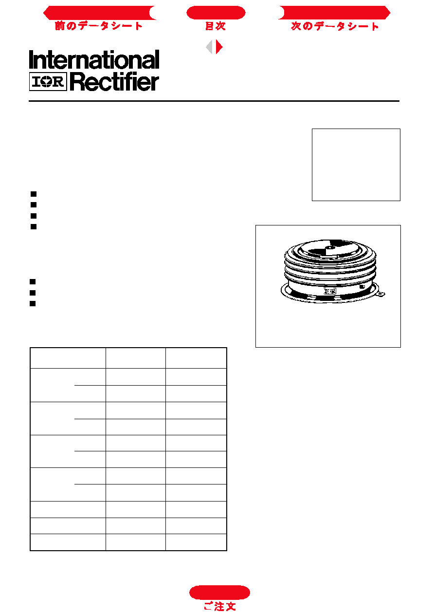
PHASE CONTROL THYRISTORS
Hockey Puk Version
ST1200C..K SERIES
Bulletin I25196/A
Features
Center amplifying gate
Metal case with ceramic insulator
International standard case A-24 (K-PUK)
High profile hockey-puk
Typical Applications
DC motor controls
Controlled DC power supplies
AC controllers
I
T(AV)
1650
A
@ T
hs
55
°C
I
T(RMS)
3080
A
@ T
hs
25
°C
I
TSM
@
50Hz
30500
A
@ 60Hz
32000
A
I
2
t
@
50Hz
4651
KA
2
s
@ 60Hz
4250
KA
2
s
V
DRM
/V
RRM
1200 to 2000
V
t
q
typical
200
µs
T
J
- 40 to 125
°C
Parameters
ST1200C..K
Units
Major Ratings and Characteristics
case style A-24 (K-PUK)
Next Data Sheet
Index
Previous Datasheet
To Order
ST1200C..K Series
Voltage
V
DRM
/V
RRM
, max. repetitive
V
RSM
, maximum non-
I
DRM
/I
RRM
max.
Type number
Code
peak and off-state voltage
repetitive peak voltage
@ T
J
= T
J
max
V
V
mA
12
1200
1300
14
1400
1500
16
1600
1700
18
1800
1900
20
2000
2100
ELECTRICAL SPECIFICATIONS
Voltage Ratings
I
T(AV)
Max. average on-state current
1650 (700)
A
180° conduction, half sine wave
@ Heatsink temperature
55 (85)
°C
double side (single side) cooled
I
T(RMS)
Max. RMS on-state current
3080
DC @ 25°C heatsink temperature double side cooled
I
TSM
Max. peak, one-cycle
30500
t = 10ms
No voltage
non-repetitive surge current
32000
A
t = 8.3ms
reapplied
25700
t = 10ms
100% V
RRM
26900
t = 8.3ms
reapplied
Sinusoidal half wave,
I
2
t
Maximum I
2
t for fusing
4651
t = 10ms
No voltage
Initial T
J
= T
J
max.
4250
t = 8.3ms
reapplied
3300
t = 10ms
100% V
RRM
3000
t = 8.3ms
reapplied
I
2
t
Maximum I
2
t for fusing
46510
KA
2
s
t = 0.1 to 10ms, no voltage reapplied
V
T(TO)
1
Low level value of threshold
voltage
V
T(TO)
2
High level value of threshold
voltage
r
t1
Low level value of on-state
slope resistance
r
t2
High level value of on-state
slope resistance
V
TM
Max. on-state voltage
1.73
V
I
pk
= 4000A, T
J
= T
J
max, t
p
= 10ms sine pulse
I
H
Maximum holding current
600
I
L
Typical latching current
1000
0.91
(16.7% x
x I
T(AV)
< I <
x I
T(AV)
), T
J
= T
J
max.
0.21
(16.7% x
x I
T(AV)
< I <
x I
T(AV)
), T
J
= T
J
max.
0.19
(I >
x I
T(AV)
),T
J
= T
J
max.
Parameter
ST1200C..K
Units Conditions
1.01
(I >
x I
T(AV)
),T
J
= T
J
max.
On-state Conduction
KA
2
s
V
m
mA
T
J
= 25°C, anode supply 12V resistive load
ST1200C..K
100
Next Data Sheet
Index
Previous Datasheet
To Order
ST1200C..K Series
di/dt
Max. non-repetitive rate of rise
Gate drive 20V, 20
, t
r
1µs
of turned-on current
T
J
= T
J
max, anode voltage
80% V
DRM
Gate current 1A, di
g
/dt = 1A/µs
V
d
= 0.67% V
DRM
,
T
J
= 25°C
I
TM
= 550A, T
J
= T
J
max, di/dt
= 40A/µs, V
R
= 50V
dv/dt
= 20V/µs, Gate 0V 100
,
t
p
= 500µs
Parameter
ST1200C..K
Units Conditions
Switching
1000
A/µs
t
d
Typical delay time
1.9
t
q
Typical turn-off time
200
µs
dv/dt
Maximum critical rate of rise of
off-state voltage
I
RRM
Max. peak reverse and off-state
I
DRM
leakage current
Blocking
500
V/µs
T
J
= T
J
max. linear to 80% rated V
DRM
Parameter
ST1200C..K
Units Conditions
100
mA
T
J
= T
J
max, rated V
DRM
/V
RRM
applied
P
GM
Maximum peak gate power
16
T
J
= T
J
max, t
p
5ms
P
G(AV)
Maximum average gate power
3
T
J
= T
J
max, f = 50Hz, d% = 50
I
GM
Max. peak positive gate current
3.0
A
T
J
= T
J
max, t
p
5ms
+V
GM
Maximum peak positive
gate voltage
-V
GM
Maximum peak negative
gate voltage
T
J
= - 40°C
mA
T
J
= 25°C
T
J
= 125°C
T
J
= - 40°C
V
T
J
= 25°C
T
J
= 125°C
I
GD
DC gate current not to trigger
10
mA
Parameter
ST1200C..K
Units Conditions
20
5.0
Triggering
TYP.
MAX.
200
-
100
200
50
-
1.4
-
1.1
3.0
0.9
-
V
GD
DC gate voltage not to trigger
0.25
V
Max. gate current/voltage not to
trigger is the max. value which
will not trigger any unit with rated
V
DRM
anode-to-cathode applied
T
J
= T
J
max
Max. required gate trigger/ cur-
rent/ voltage are the lowest value
which will trigger all units 12V
anode-to-cathode applied
V
GT
DC gate voltage required
to trigger
I
GT
DC gate current required
to trigger
W
V
T
J
= T
J
max, t
p
5ms
To Order
Next Data Sheet
Index
Previous Datasheet
ST1200C..K Series
T
J
Max. operating temperature range
-40 to 125
T
stg
Max. storage temperature range
-40 to 150
R
thJ-hs
Max. thermal resistance,
0.042
DC operation single side cooled
junction to heatsink
0.021
DC operation double side cooled
R
thC-hs
Max. thermal resistance,
0.006
DC operation single side cooled
case to heatsink
0.003
DC operation double side cooled
F
Mounting force, ± 10%
24500
N
(2500)
(Kg)
wt
Approximate weight
425
g
Parameter
ST1200C..K
Units
Conditions
K/W
°C
Case style
A-24 (K-PUK)
See Outline Table
K/W
Thermal and Mechanical Specification
Single Side Double Side
Single Side Double Side
180°
0.003
0.003
0.002
0.002
T
J
= T
J
max.
120°
0.004
0.004
0.004
0.004
90°
0.005
0.005
0.005
0.005
K/W
60°
0.007
0.007
0.007
0.007
30°
0.012
0.012
0.012
0.012
Sinusoidal conduction
Rectangular conduction
Conduction angle
Units
Conditions
R
thJ-hs
Conduction
(The following table shows the increment of thermal resistence R
thJ-hs
when devices operate at different conduction angles than DC)
1
-
Thyristor
2
-
Essential part number
3
-
0 = Converter grade
4
-
C = Ceramic Puk
5
-
Voltage code: Code x 100 = V
RRM
(See Voltage Rating Table)
6
-
K = Puk Case A-24 (K-PUK)
7
-
0 = Eyelet terminals (Gate and Auxiliary Cathode Unsoldered Leads)
1 = Fast-on terminals (Gate and Auxiliary Cathode Unsoldered Leads)
2 = Eyelet terminals (Gate and Auxiliary Cathode Soldered Leads)
3 = Fast-on terminals (Gate and Auxiliary Cathode Soldered Leads)
8
-
Critical dv/dt: None = 500V/µsec (Standard selection)
L
= 1000V/µsec (Special selection)
Ordering Information Table
Device Code
5
1
2
3
4
ST 120
0
C
20
K
1
7
6
8
To Order
Next Data Sheet
Index
Previous Datasheet
ST1200C..K Series
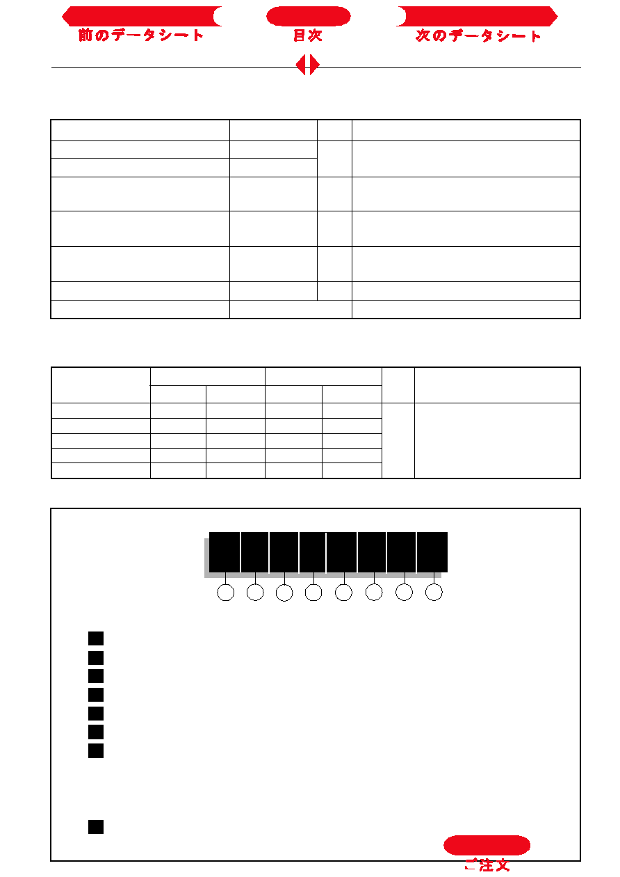
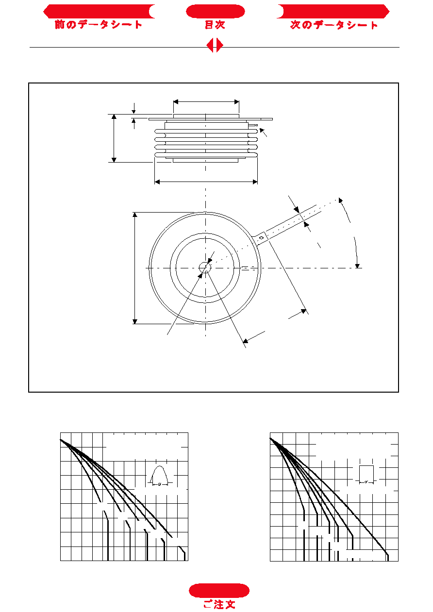
Outline Table
Fig. 1 - Current Ratings Characteristics
Fig. 2 - Current Ratings Characteristics
40
50
60
70
80
90
100
110
120
130
0
200
400
600
800
1000
1200
30°
60°
90°
120°
180°
Average On-state Current (A)
Conduc tion Angle
M
a
x
i
m
u
m
A
l
l
o
w
abl
e H
eat
s
i
n
k
T
e
m
p
e
r
at
u
r
e
(
°
C
)
ST1200C..K Series
(Single Side Cooled )
R (DC) = 0.042 K/ W
thJ-hs
20
30
40
50
60
70
80
90
100
110
120
130
0
400
800
1200
1600
2000
DC
30°
60°
90°
120°
180°
Average On-state Current (A)
Conduction Period
M
a
x
i
m
u
m
A
l
l
o
w
a
bl
e H
e
at
s
i
nk
T
em
pe
r
a
t
u
r
e
(
°
C
)
ST1200C..K Series
(Single Side Cooled)
R (DC) = 0.042 K/ W
thJ-hs
Case Style A-24 (K-PUK)
All dimensions in millimeters (inches)
TWO PLACES
PIN RECEPTACLE
AMP. 60598-1
1 (0.04) MIN.
TWO PLACES
47.5 (1.87) DIA. MAX.
7
4
.5
(
2
.9
)
D
I
A
.
M
A
X
.
2 HOLES DIA. 3.5 (0.14) x
2.1 (0.1) DEEP
4.75 (0.2) NOM.
27.
5
(
1
.
0
8)
M
A
X
.
20° ± 5°
44 (1.73)
CREPAGE DESTANCE 28.88 (1.137) MIN.
STRIKE DISTANCE 17.99 (0.708) MIN.
67 (2.6) DIA. MAX.
To Order
Next Data Sheet
Index
Previous Datasheet