3360A
PHASE CONTROL THYRISTORS
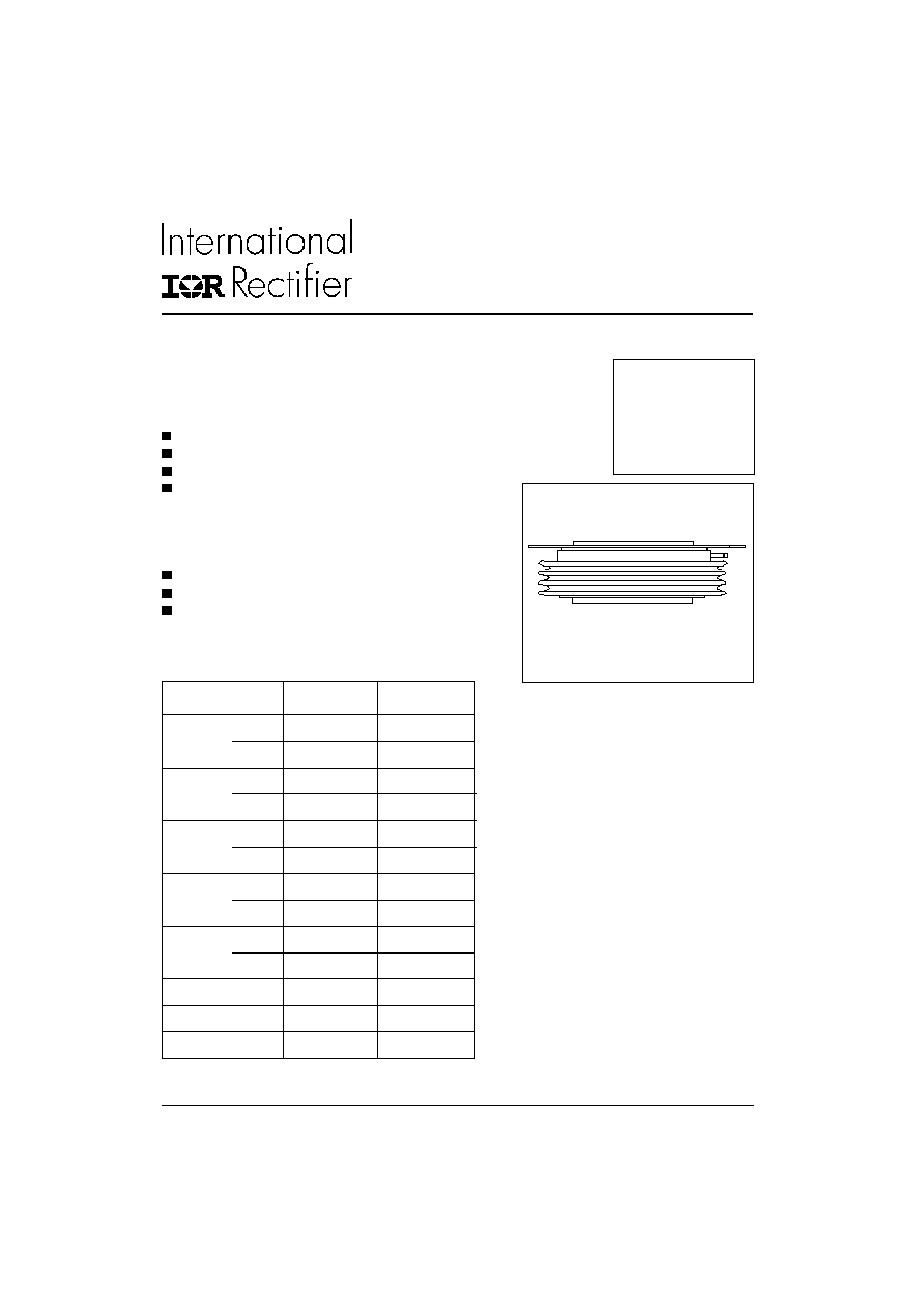
Hockey Puk Version
ST3230C..R SERIES
1
Bulletin I25200 rev. B 04/00
www.irf.com
Features
Double side cooling
High surge capability
High mean current
Fatigue free
Typical Applications
DC motor controls
Controlled DC power supplies
AC controllers
I
T(AV)
2785
A
@ T
C
80
∞C
I
T(AV)
3360
A
@ T
hs
55
∞C
I
T(RMS)
5970
A
@ T
hs
25
∞C
I
TSM
@
50Hz
61200
A
@
60Hz
64000
A
I
2
t
@
50Hz
18730
KA
2
s
@
60Hz
17000
KA
2
s
V
DRM
/V
RRM
1000 to 1800
V
t
q
typical
500
µs
T
J
max.
125
∞C
Parameters
ST3230C..R
Units
Major Ratings and Characteristics
(R-PUK)
ST3230C..R Series
2
Bulletin I25200 rev. B 04/00
www.irf.com
Voltage
V
DRM
/V
RRM
, max. repetitive
V
RSM
, maximum non-
I
DRM
/I
RRM
max.
Type number
Code
peak and off-state voltage
repetitive peak voltage
@ T
C
= 125∞C
V
V
mA
10
1000
1100
12
1200
1300
14
1400
1500
16
1600
1700
18
1800
1900
ELECTRICAL SPECIFICATIONS
Voltage Ratings
I
T(AV)
Max. average on-state current
2785 (1720)
A
@ Case temperature
80
∞C
I
T(AV)
Max. average on-state current
3360 (1360)
A
@ Heatsink temperature
55 (85)
∞C
I
T(RMS)
Max. RMS on-state current
5970
A
DC @ 25∞C heatsink temperature double side cooled
I
TSM
Max. peak, one-cycle
No voltage
non-repetitive surge current
reapplied
50% V
RRM
reapplied
Sinusoidal half wave,
I
2
t
Maximum I
2
t for fusing
No voltage
Initial T
C
= 125∞C
reapplied
50% V
RRM
reapplied
V
T(TO)
Max. value of threshold voltage
0.92
V
T
J
= T
J
max.
r
t
Max. value of on-state slope
resistance
V
TM
Max. on-state voltage
1.3
V
I
pk
= 2900A, T
C
= 25∞C
I
L
Typical latching current
300
mA
T
J
= 25∞C, V
D
=
5V
Parameter
ST3230C..R
Units
Conditions
On-state Conduction
A
KA
2
s
0.09
T
J
= T
J
max.
m
180∞ conduction, half sine wave
double side (single side [anode side]) cooled
Parameter
ST3230C..R
Units Conditions
di/dt
Max. repetitive 50Hz (no repetitive)
From 67% V
DRM
to 1000A gate drive 10V, 5
, t
r
= 0.5µs
rate of rise of turned-on current
to 1A, T
J
= T
J
max.
Gate drive 30V, 15
,
V
d
= 67% V
DRM
,
T
J
= 25∞C
Rise time 0.5µs
I
T
= 1000A, t
p
= 1ms, T
J
= T
J
max, V
RM
= 50V,
dI
RR
/dt = 2A/µs, V
DR
=
67% V
DRM
,
dv
DR
/dt
= 8V/µs linear
150 (300)
A/µs
µs
t
q
Typical turn-off time
500
t
d
Maximum delay time
4.5
t = 10ms
t = 8.3ms
t = 10ms
t = 8.3ms
t = 10ms
t = 8.3ms
t = 10ms
t = 8.3ms
61200
64000
49000
51300
18730
17000
12000
10920
ST3230C..R
250
Switching
ST3230C..R Series
3
Bulletin I25200 rev. 04/00
www.irf.com
dv/dt
Maximum linear rate of rise of
off-state voltage
I
RRM
Max. peak reverse and off-state
I
DRM
leakage current
500
V/µs
T
J
= T
J
max. to 67% rated V
DRM
Parameter
ST3230C..R
Units
Conditions
250
mA
T
J
= 125∞C rated V
DRM
/V
RRM
applied
Triggering
P
GM
Maximum peak gate power
150
t
p
= 100µs
P
G(AV)
Maximum average gate power
10
I
GM
Max. peak positive gate current
30
A
Anode positive with respect to cathode
V
GM
Max. peak positive gate voltage
30
V
Anode positive with respect to cathode
-V
GM
Max. peak negative gate voltage
0.25
V
Anode negative with respect to cathode
I
GT
Maximum DC gate current
required to trigger
V
GT
Maximum gate voltage required
to trigger
Parameter
ST3230C..R
Units
Conditions
W
400
mA
T
C
= 25∞C, V
DRM
= 5V
4
V
T
C
= 25∞C, V
DRM
= 5V
V
GD
DC gate voltage not to trigger
0.25
V
T
C
= 125∞C
Max. gate current/voltage not to
trigger is the max. value which
will not trigger any unit with rated
V
DRM
anode-to-cathode applied
180∞
0.0010
0.0010
T
J
= T
J
max.
120∞
0.0017
0.0017
K/W
60∞
0.0044
0.0044
R
thJ-C
Conduction
(The following table shows the increment of thermal resistence R
thJ-C
when devices operate at different conduction angles than DC)
Conduction angle
Single side
Double side
Units
Conditions
T
J
max. Max. operating temperature
125
On-state (conducting)
T
stg
Max. storage temperature range
-55 to 125
R
thJ-C
Thermal resistance, junction
0.019
DC operation single side cooled
to case
0.0095
DC operation double side cooled
R
th(C-h)
Thermal resistance, case
0.004
Single side cooled
to heatsink
0.002
Double side cooled
F
Mounting force ± 10%
wt
Approximate weight
1600
g
Case style
(R-PUK)
See Outline Table
Parameter
ST3230C..R
Units
Conditions
Thermal and Mechanical Specification
∞C
Clamping force 43KN with
mounting compound
43000
(4400)
N
(Kg)
Blocking
K/W
K/W
ST3230C..R Series
4
Bulletin I25200 rev. B 04/00
www.irf.com
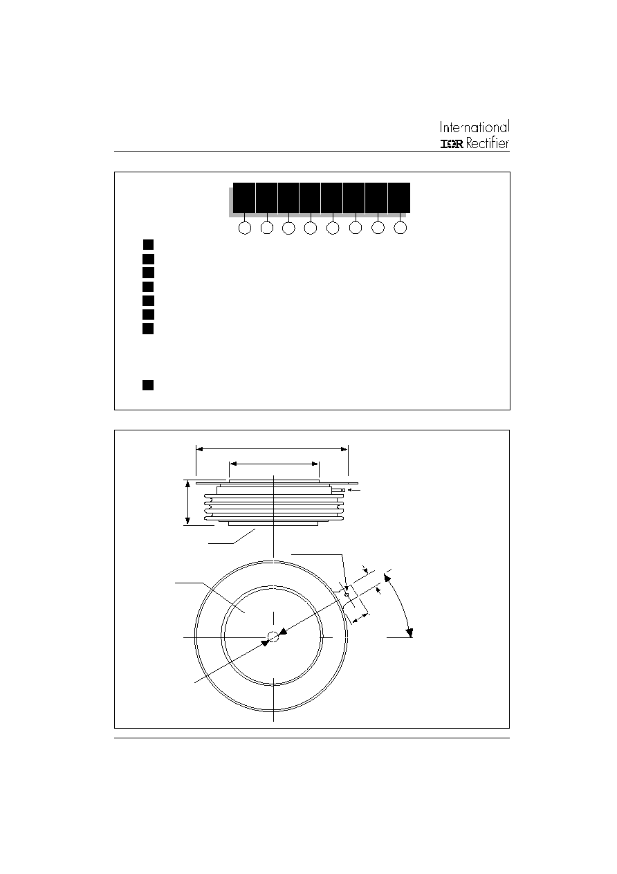
Ordering Information Table
Device Code
5
1
2
3
4
ST 323
0
C
18
R
1
7
6
8
1
-
Thyristor
2
-
Essential part number
3
-
0 = Converter grade
4
-
C = Ceramic Puk
5
-
Voltage code: Code x 100 = V
RRM
(See Voltage Rating Table)
6
-
R = Puk Case
7
-
0 = Eyelet terminals (Gate and Auxiliary Cathode Unsoldered Leads)
1 = Fast-on terminals (Gate and Auxiliary Cathode Unsoldered Leads)
2 = Eyelet terminals (Gate and Auxiliary Cathode Soldered Leads)
3 = Fast-on terminals (Gate and Auxiliary Cathode Soldered Leads)
8
-
Critical dv/dt: None = 500V/µsec (Standard selection)
L
= 1000V/µsec (Special selection)
Outline Table
(R-PUK)
All dimensions in millimeters (inches)
112.5 (4.4) DIA. MAX.
73.2 (2.9) DIA. MAX.
TWO PLACES
GATE
1.5 (0.06) DIA.
3
7
.7
(
1
.5
)
M
A
X
.
ANODE
3.7 (0.15) DIA. NOM. X
2.1 (0.1) DEEP MIN.
BOTH ENDS
CATHODE
HOLE 1.5 (0.06)
DIA. MAX.
4.76 (0.2)
20∞ ± 5∞
6 .3
(0
. 2
4 )
Quote between upper and lower
pole pieces has to be considered
after application of Mounting Force
(see Thermal and Mechanical
Specification)

ST3230C..R Series
5
Bulletin I25200 rev. B 04/00
www.irf.com
Fig. 1 - Current Ratings Characteristics
Fig. 2 - Current Ratings Characteristics
Fig. 5 - Maximum Non-Repetitive Surge Current
Fig. 6 - Maximum Non-Repetitive Surge Current
Fig. 4 - On-state Voltage Drop Characteristics
2 0
3 0
4 0
5 0
6 0
7 0
8 0
9 0
1 0 0
1 1 0
1 2 0
1 3 0
0
5 0 0 1 0 0 0 1 5 0 0 2 0 0 0 2 5 0 0 3 0 0 0 3 5 0 0
6 0 ∞
1 2 0 ∞
1 8 0 ∞
A v e ra g e O n -st a te C u rre n t (A )
Co nd uctio n A ng le
M
a
xi
m
u
m
A
l
l
o
w
a
bl
e
He
at
s
i
n
k
T
e
m
p
e
r
at
u
r
e
(
∞
C
)
D C
ST 3 2 3 0 C ..R Se rie s
( Sin g le Sid e C o o le d )
R ( D C ) = 0 .0 2 3 K / W
th J -hs
2 0
3 0
4 0
5 0
6 0
7 0
8 0
9 0
1 0 0
1 1 0
1 2 0
1 3 0
0
1 0 00
2 0 00
3 00 0
4 0 00
5 0 00
60 0 0
60∞
12 0∞
18 0∞
Average O n-state Curren t (A)
C o nd u c tio n A ng le
M
a
x
i
m
u
m
A
l
l
o
w
a
bl
e
He
at
s
i
n
k
T
e
mpe
r
at
u
r
e
(
∞
C)
ST3230 C..R Ser ies
(D ouble Side Cooled)
R (DC) = 0.011 5 K/W
th J -hs
DC
0
1 0 00
2 0 00
3 0 00
4 0 00
5 0 00
6 0 00
7 0 00
8 0 00
9 0 00
0
1 00 0
2 0 00
3 0 00
40 0 0
5 0 00
6 00 0
RMS Lim it
Co n d uc tion Ang le
M
a
x
i
mu
m A
v
e
r
a
g
e
O
n
-
s
t
a
t
e
P
o
w
e
r
L
o
s
s
(
W
)
Average O n-state Curren t (A)
ST32 30C..R Series
T = 125 ∞C
J
D C
18 0∞
12 0∞
6 0∞
Fig. 3 - On-state Power Loss Characteristics
1 0 0
1 0 0 0
1 0 0 0 0
0 .5
1
1 . 5
2
I
n
s
t
a
n
ta
n
e
o
u
s
O
n
-
s
t
a
te
C
u
r
r
e
n
t
(
A
)
In sta n t a n e o u s O n - st a te V o lt a g e ( V )
T = 1 2 5 ∞ C
J
S T3 2 3 0 C ..R Se rie s
1 5 0 0 0
2 0 0 0 0
2 5 0 0 0
3 0 0 0 0
3 5 0 0 0
4 0 0 0 0
4 5 0 0 0
5 0 0 0 0
5 5 0 0 0
1
1 0
1 0 0
N um b e r O f E q u a l Am p litud e H a lf C yc le C urre n t Pulse s (N )
P
e
ak
Hal
f
S
i
n
e
W
a
v
e
O
n
-
s
t
a
t
e
C
u
r
r
e
n
t
(
A
)
In it ia l T = 1 2 5 ∞C
@ 6 0 H z 0 .0 0 8 3 s
@ 5 0 H z 0 .0 1 0 0 s
J
ST 3 2 3 0 C ..R Se rie s
A t A n y R a t e d L o a d C o n d it io n A n d W it h
5 0 % R a t e d V A p p lie d Fo llo w in g S u rg e
RR M
4 0 0 00
5 0 0 00
6 0 0 00
7 0 0 00
8 0 0 00
9 0 0 00
1 0 0 0 0 0
1
1 0
M a xim u m N o n R e pe t it iv e Su rg e C u rre n t
V e rsu s P u lse T ra in D u ra t io n . C o n t ro l
O f C o n d u c tio n M a y N o t Be M a in ta in e d .
P
e
ak
Hal
f
S
i
n
e
W
a
v
e
O
n
-
s
t
a
t
e
C
u
r
r
e
n
t
(
A
)
5 0 % R a t e d V R e a p p lie d
R RM
S T 3 2 3 0 C ..R Se rie s
In itia l T = 1 2 5 ∞C
J
Pu lse Tr a in D u ra t io n ( m s)
ST3230C..R Series
6
Bulletin I25200 rev. B 04/00
www.irf.com
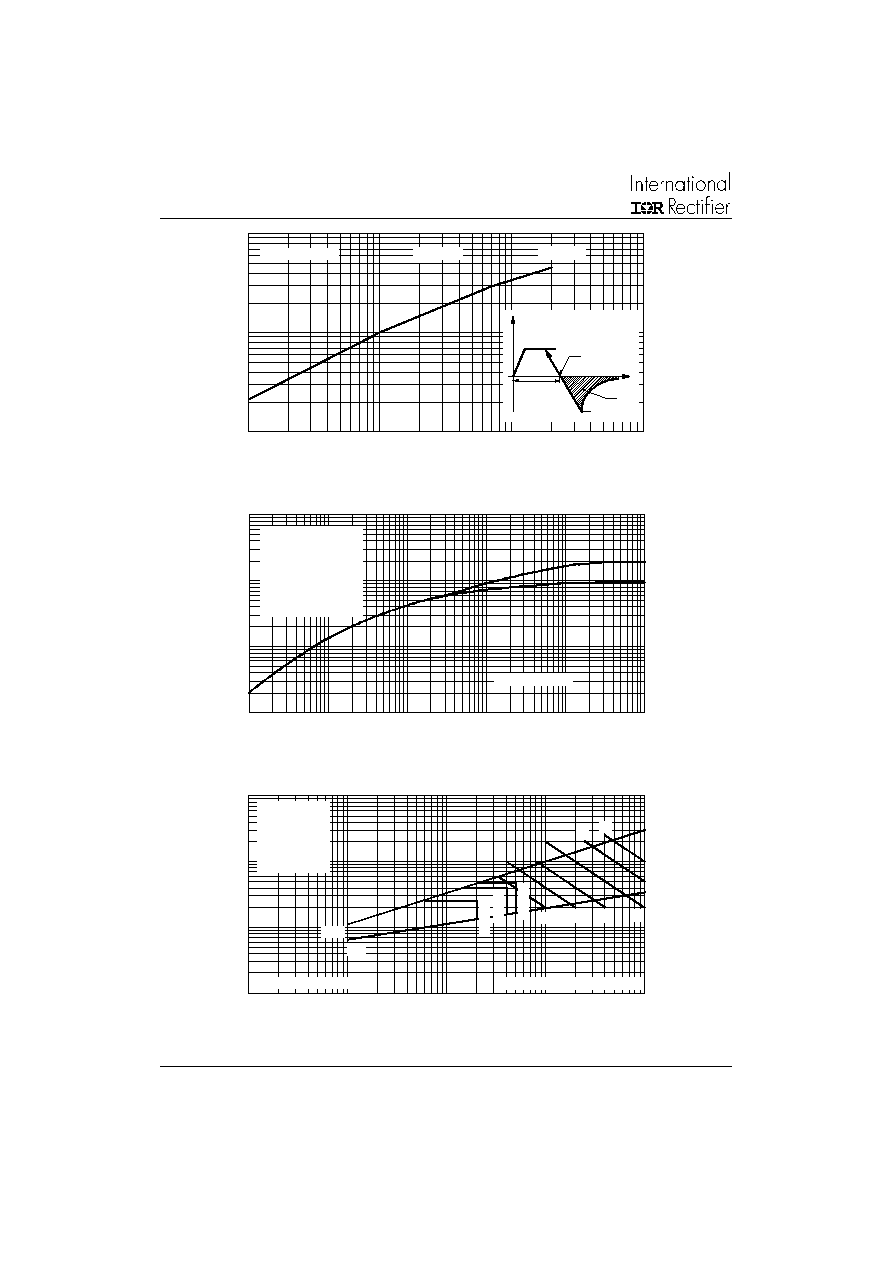
Fig. 7 - Stored Charged
Fig. 8 - Thermal Impedance Z
thJ-C
Characteristics
Fig. 9 - Gate Characteristics
1 0 0
1 0 0 0
1 0 0 0 0
0 . 1
1
1 0
1 0 0
T
o
t
a
l
s
t
o
r
e
d
c
h
a
r
g
e
-
Q
rr
(
µ
C
)
Ra t e O f D e c a y O f O n - sta t e C u rre n t - d i/ d t ( A / µ s)
T = 1 2 5 ∞ C
J
S T 3 2 3 0 C .. R Se rie s
I = 1 0 0 0 A
T
Q
r r
I
T
dI
I ( REC )
RM
t
d t
T
t = 3 ms
p
0 . 0 0 0 1
0 . 0 0 1
0 . 0 1
0 . 1
0 .0 0 1
0 . 0 1
0 . 1
1
1 0
1 0 0
Sq u are W a v e P ulse D u ra t io n ( s)
St e ad y St a t e V a lu e
R = 0 . 0 1 9 K / W
( Sin g le Sid e C o o le d )
R = 0 . 0 0 9 5 K/ W
( D o u b le S id e C o o le d )
( D C O p e rat io n )
thJ -C
thJ -C
th
J
-
C
T
r
a
n
s
i
e
n
t
T
h
e
r
m
a
l
I
m
p
e
d
a
n
c
e
Z
(
K
/
W
)
ST 3 2 3 0 C .. R S e rie s
0 . 1
1
1 0
1 0 0
0 . 0 0 1
0 . 0 1
0 .1
1
1 0
V G D
IG D
Tj
=
2
5
∞
C
T
j
=
1
25
∞
C
Tj
=
-
4
0
∞
C
( 1 )
( 2 )
In sta n ta n e o u s G a te C u rre n t ( A )
I
n
st
an
t
a
n
e
o
u
s G
a
t
e
V
o
l
t
ag
e
(
V
)
F re q u e n c y L im ite d b y P G ( A V )
( 1 ) PG M = 2 W
( 2 ) PG M = 4 W
( 3 ) PG M = 8 W
( 4 ) PG M = 2 0 W
( 5 ) PG M = 5 0 W
( 6 ) PG M = 1 0 0 W
D e v ic e : S T3 2 3 0 C . .R Se rie s
( 3 )
( 4 )
( 5 )
( 6 )