IS42G32256
Integrated Silicon Solution, Inc.
1
ADVANCE INFORMATION SR037-0C
09/10/98
ISSI
Æ
This document contains ADVANCE INFORMATION data. ISSI reserves the right to make changes to its products at any time without notice in order to improve design and supply the best possible
product. We assume no responsibility for any errors which may appear in this publication. © Copyright 1998, Integrated Silicon Solution, Inc.
FEATURES
∑ 256,144 words x 32 bits x 2-bank organization
∑ All inputs are sampled at the positive going
edge of the system clock
∑ Dual internal bank control
∑ Single 3.3V
±
3V power supply
∑ Programmable mode register
≠ Burst length (1, 2, 4, 8, and full page)
≠ CAS latency (2 and 3)
≠ Burst type: Sequential and Interleave
∑ Burst Read single-bit Write Operation
∑ Refresh capability
≠ Auto, self-refresh
∑ 2,048 refresh cycles/32 ms
∑ LVTTL compatible inputs and outputs
∑ 100-pin PQFP
(14mm x 20mm)
DESCRIPTION
The ISSI IS42G32256 is a high-speed 16-Mbit CMOS
Synchronous Graphics RAM organized as 256K words x
32 bits x 2 banks. With SGRAM, all input and output
signals are synchronized with the rising edge of the
system clock. Programmable Mode Register and
Special Registers provide a choice of Read or Write burst
lengths of 1, 2, 4, or 8 locations or a Full Page with burst
termination options. The SGRAM performance is
enhanced with the Write-per-bit (WPB) and eight columns
of Block Write functions.
The IS42G32256 is ideal for high-performance, high-
bandwidth applications including workstation graphics,
set top box, games, and PC-2D/3D graphic applications.
IS42G32256
256K x 32 x 2 (16-Mbit)
SYNCHRONOUS GRAPHICS RAM
ADVANCE INFORMATION
SEPTEMBER 1998
Table 1. Key Timing Parameters
Symbol
Parameter
-7
-8
-10
Units
t
CK
Clock Cycle Time
7
8
10
ns
Access Time @ CL = 3
6
6.5
7
ns
Operating Frequency
143
125
100
MHz
GRAPHIC FEATURES
∑ SMRS cycle
≠ Load mask register
≠ Load color register
∑ Write per bit (old mask)
∑ Block write (eight columns)
ISSI
Æ

IS42G32256
2
Integrated Silicon Solution, Inc.
ADVANCE INFORMATION SR037-0C
09/10/98
ISSI
Æ
CLK
CKE
CS
RAS
CAS
WE
DSF
DQM0-3
PROGRAM
REGISTER
TIMING
REGISTER
LA
TENCY
&
BURST
LENGTH
COLUMN
DECODER
MASK
SENSE
AMPLIFIER
256K x 32
MEMORY
CELL
ARRAY
256K x 32
MEMORY
CELL
ARRAY
ROW DECODER
INPUT REGISTER
ROW
ADDRESS BUFFER
REFRESH
COUNTER
WRITE
CONTROL
LOGIC
DQM0-3
BLOCK
WRITE
CONTROL
LOGIC
COLUMN
MASK
MUX
COLOR
REGISTER
MASK
REGISTER
COLUMN
ADDRESS BUFFER
SERIAL
COUNTER
A0-A10
CLOCK
DATA IN
BUFFER
DATA OUT
BUFFER
DQ31-DQ0
DQM0-3
Figure 1. IS42G32256 Functional Block Diagram

IS42G32256
Integrated Silicon Solution, Inc.
3
ADVANCE INFORMATION SR037-0C
09/10/98
ISSI
Æ
Figure 2. IS42G32256 Pin Configuration, 100-pin PQFP
DQ28
V
CCQ
DQ27
DQ26
GND
Q
DQ25
DQ24
V
CCQ
DQ15
DQ14
GND
Q
DQ13
DQ12
V
CCQ
GND
V
CC
DQ11
DQ10
GND
Q
DQ9
DQ8
V
CCQ
NC
DQM3
DQM1
CLK
CKE
DSF
NC
A9
DQ2
GND
Q
DQ1
DQ0
V
CC
NC
NC
NC
NC
NC
NC
NC
NC
NC
NC
GND
DQ31
DQ30
GND
Q
DQ29
DQ3
V
CCQ
DQ4
DQ5
GND
Q
DQ6
DQ7
V
CCQ
DQ16
DQ17
GND
Q
DQ18
DQ19
V
CCQ
V
CC
GND
DQ20
DQ21
GND
Q
DQ22
DQ23
V
CCQ
DQM0
DQM2
WE
CAS
RAS
CS
BA (A10)
A8
1
2
3
4
5
6
7
8
9
10
11
12
13
14
15
16
17
18
19
20
21
22
23
24
25
26
27
28
29
30
80
79
78
77
76
75
74
73
72
71
70
69
68
67
66
65
64
63
62
61
60
59
58
57
56
55
54
53
52
51
100 99 98 97 96 95 94 93 92 91 90 89 88 87 86 85 84 83 82 81
31 32 33 34 35 36 37 38 39 40 41 42 43 44 45
A0
A1
A2
A3
V
CC
NC
NC
NC
NC
NC
NC
NC
NC
NC
NC
GND
A4
A5
A6
A7
46 47 48 49 50
IS42G32256
4
Integrated Silicon Solution, Inc.
ADVANCE INFORMATION SR037-0C
09/10/98
ISSI
Æ
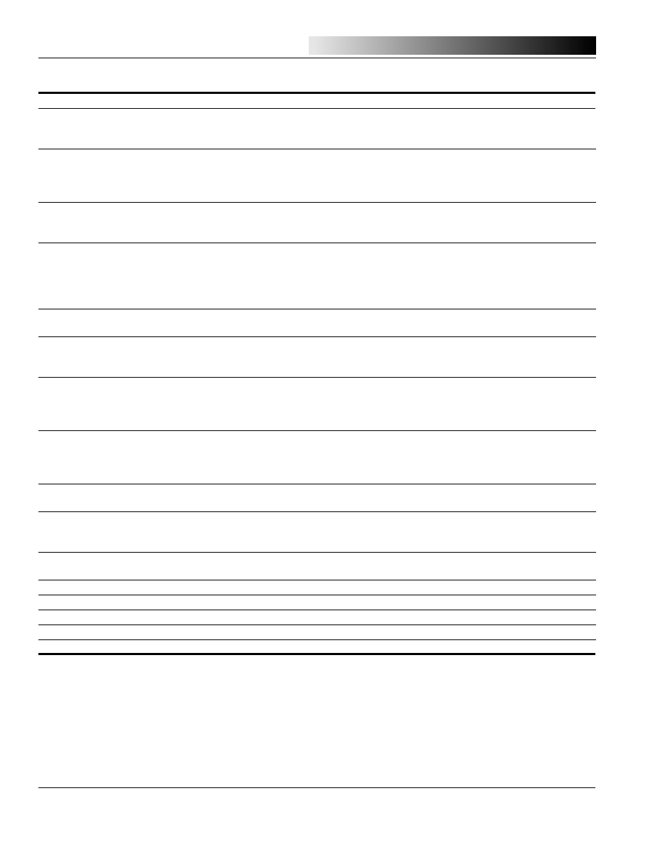
Table 2. Pin Descriptions
Symbol
Pin Number
I/O
Name and Function
A0-A9
30-34, 47-51
I
Address: Row/Column addresses are multi-
plexed on the same pins. Row address: RA0-
RA9
Column address: CA0-CA7
A10/BP
29
I
Bank Select Address: Selects bank to be acti-
vated during row address latch time. Selects
bank for read/write during column address latch
time.
CAS
26
I
Column Address Strobe: Latches column ad-
dresses on the positive going edge of the CLK
with
CAS
low. Enables column access.
CKE
54
I
Clock Enable: Masks system clock to freeze
operation from the next clock cycle. CKE should
be enabled at least one clock + t
CKS
prior to new
command. Disable input buffers for power down
in standby.
CLK
55
I
System Clock: Active on the positive going
edge to sample all inputs.
CS
28
I
Chip Select: Disables or enables device opera-
tion by masking or enabling all inputs except
CLK, CKE and DQM
X
.
DQ0-DQ31
1, 3-4, 6-7, 9-10,
I/O
Data Input/Output: Data Inputs/Outputs are
12-13, 17-18, 20-21, 60-61,
multiplexed on the same pins.
63-64, 68-69, 71-72, 74-75,
77-78, 81-81, 83-84, 97-98, 100
DQM0-DQM3
23-24, 56-57
I/O
Data Input/Output Mask: Makes data output
Hi-Z, t
SHZ
after the clock and masks the output.
Blocks data input when DQM active. (Byte Mask-
ing)
DSF
53
Define Special Function: Enables write per bit,
block write and special mode register set.
RAS
27
I
Row Address Strobe: Latches row addresses
on the positive going edge of the CLK with
RAS
low. Enables row access and precharge.
WE
25
I
Write Enable: Enables write operation and row
precharge.
V
CCQ
2, 8, 14, 22, 59, 67, 73, 76, 79
Supplies voltage for data output
Vcc
15, 35, 65, 96
Power Supply Voltage
GND
Q
5, 11, 19, 62, 70, 82, 99
Ground for D
Q
GND
16, 46, 66, 85
Ground
NC
36-45, 52, 58, 86-95
No connect

IS42G32256
Integrated Silicon Solution, Inc.
5
ADVANCE INFORMATION SR037-0C
09/10/98
ISSI
Æ
Table 3. Frequency vs. AC Parameter Relationships
IS42G32256: 7 ns (Unit: number of clocks)
CAS
CAS
CAS
CAS
CAS
t
RC
t
RAS
t
RP
t
RRD
t
RCD
t
CCD
t
CDL
t
RDL
Frequency
Latency
63 ns
42 ns
21 ns
14 ns
20 ns
7 ns
7 ns
7 ns
143 MHz (7 ns)
3
9
6
3
2
3
1
1
1
125 MHz (8 ns)
3
8
6
3
2
3
1
1
1
100 MHz (10 ns)
2
7
5
3
2
2
1
1
1
83 MHz (12 ns)
2
6
4
2
2
2
1
1
1
75 MHz (13.4 ns)
2
5
4
2
2
2
1
1
1
66 MHz (15 ns)
2
5
3
2
1
2
1
1
1
IS42G32256: 8 ns (Unit: number of clocks)
CAS
CAS
CAS
CAS
CAS
t
RC
t
RAS
t
RP
t
RRD
t
RCD
t
CCD
t
CDL
t
RDL
Frequency
Latency
70 ns
48 ns
24 ns
16 ns
20 ns
8 ns
8 ns
8 ns
125 MHz (8 ns)
3
9
6
3
2
3
1
1
1
100 MHz (10 ns)
3
8
5
3
2
2
1
1
1
83 MHz (12 ns)
2
6
4
2
2
2
1
1
1
75 MHz (13.4 ns)
2
6
4
2
2
2
1
1
1
66 MHz (15 ns)
2
5
4
2
2
2
1
1
1
50 MHz (20 ns)
2
4
3
2
1
1
1
1
1
IS42G32256: 10 ns (Unit: number of clocks)
CAS
CAS
CAS
CAS
CAS
t
RC
t
RAS
t
RP
t
RRD
t
RCD
t
CCD
t
CDL
t
RDL
Frequency
Latency
80 ns
50 ns
26 ns
20 ns
20 ns
10 ns
10 ns
10 ns
100 MHz (10 ns)
3
8
5
3
2
2
2
1
1
83 MHz (12 ns)
3
7
5
3
2
2
2
1
1
71 MHz (14 ns)
2
6
4
2
2
2
2
1
1
66 MHz (15 ns)
2
6
4
2
2
2
2
1
1
50 MHz (20 ns)
2
4
3
2
1
1
1
1
1
40 MHz (25 ns)
2
4
2
2
1
1
1
1
1