
Integrated Silicon Solution, Inc. -- 1-800-379-4774
1
Rev. D
11/01/05
ISSI
Æ
IS42S83200A
(4-bank x 8,388,608 - word x 8-bit)
IS42S16160A
(4-bank x 4,194,304 - word x 16-bit)
256 Mb Synchronous DRAM
DESCRIPTION
IS42S83200A is a synchronous 256Mb SDRAM and is
organized as 4-bank x 8,388,608-word x 8-bit; and
IS42S16160A is organized as 4-bank x 4,194,304-word x
16-bit. All inputs and outputs are referenced to the rising
edge of CLK.
FEATURES
IS42S83200A and IS42S16160A achieve very
high speed clock rates up to 166MHz, and are
suitable for main memories or graphic
memories in computer systems.
- Single 3.3V ±0.3V power supply
- Max. Clock frequency:
-6:166MHz<3-3-3>
- Fully synchronous operation referenced to clock rising edge
- 4-bank operation controlled by BA0,BA1(Bank Address)
- /CAS latency- 2/3 (programmable)
- Burst length- 1/2/4/8/FP (programmable)
- Burst type- Sequential and interleave burst (programmable)
- Byte Control- DQML and DQMU (IS42S16160A)
- Random column access
- Auto precharge / All bank precharge controlled by A10
- Auto and self refresh
- 8192 refresh cycles /64ms(4 banks concurrent refresh)
- LVTTL Interface
- Row address A0-12 /Column address A0-9(x8) / A0-8(x16)
- Package: 400-mil, 54-pin Thin Small Outline (TSOP II) with 0.8mm lead pitch
ITEM
-6
-7
-75
Unit
tCLK
Clock Cycle Time
(Min.)
CL=2
-
-
10
ns
CL=3
6
7
7.5
ns
tRAS Active to Precharge Command Period (Min.)
42
45
45
ns
tRCD
Row to Column Delay
(Min.)
15
20
20
ns
tAC
Access Time from CLK
(Max.)
CL=2
-
-
ns
CL=3
5
5.4
5.4
ns
tRC
Ref /Active Command Period
(Min.)
60
63
67.5
ns
Icc1
Operation Current (Single Bank)
(Max.)
IS42S83200A
110
mA
IS42S16160A
130
130
mA
Icc6
Self Refresh Current
(Max.) -6,-7,-75
3
3
mA
6
3
IS42S83200A/16160A
-
-
-
- Lead-free available
-7:143MHz<3-3-3>
-75:133MHz<3-3-3>
November 2005

2
Integrated Silicon Solution, Inc. -- 1-800-379-4774
Rev. D
11/01/05
ISSI
Æ
IS42S83200A
(4-bank x 8,388,608 - word x 8-bit)
IS42S16160A
(4-bank x 4,194,304 - word x 16-bit)
PIN CONFIGURATION (TOP VIEW)
CLK
: Master Clock
CKE
: Clock Enable
/CS
: Chip Select
/RAS
: Row Address Strobe
DQM, DQMU/L : Output Disable / Write Mask
A0-12
: Address Input
BA0,1
: Bank Address Input
Vdd
: Power Supply
/CAS
: Column Address Strobe
VddQ
: Power Supply for Output
/WE
: Write Enable
Vss
: Ground
DQ0-15
: Data I/O
VssQ
: Ground for Output
x8
x16
Vdd
Vdd
Vss
Vss
DQ0
DQ0
DQ15
DQ7
VddQ
VddQ
VssQ
VssQ
NC
DQ1
DQ14
NC
DQ1
DQ2
DQ13
DQ6
VssQ
VssQ
VddQ
VddQ
NC
DQ3
DQ12
NC
DQ2
DQ4
DQ11
DQ5
VddQ
VddQ
VssQ
VssQ
NC
DQ5
DQ10
NC
DQ3
DQ6
DQ9
DQ4
VssQ
VssQ
VddQ
VddQ
NC
DQ7
DQ8
NC
Vdd
Vdd
Vss
Vss
NC
DQML
NC
NC
/WE
/WE
DQMU
DQM
/CAS
/CAS
CLK
CLK
/RAS
/RAS
CKE
CKE
/CS
/CS
A12
A12
BA0
BA0
A11
A11
BA1
BA1
A9
A9
A10/AP A10/AP
A8
A8
A0
A0
A7
A7
A1
A1
A6
A6
A2
A2
A5
A5
A3
A3
A4
A4
Vdd
Vdd
Vss
Vss
1
2
3
4
5
6
7
8
9
10
11
12
13
14
15
16
17
18
19
20
21
22
23
24
25
26
27
54
53
52
51
50
49
48
47
46
45
44
43
42
41
40
39
38
37
36
35
34
33
32
31
30
29
28
40
0mi
lx8
75m
il
54
pin
0.
8mm
pit
ch
TS
OP(I
I)
Integrated Silicon Solution, Inc. -- 1-800-379-4774
3
Rev. D
11/01/05
ISSI
Æ
IS42S83200A
(4-bank x 8,388,608 - word x 8-bit)
IS42S16160A
(4-bank x 4,194,304 - word x 16-bit)
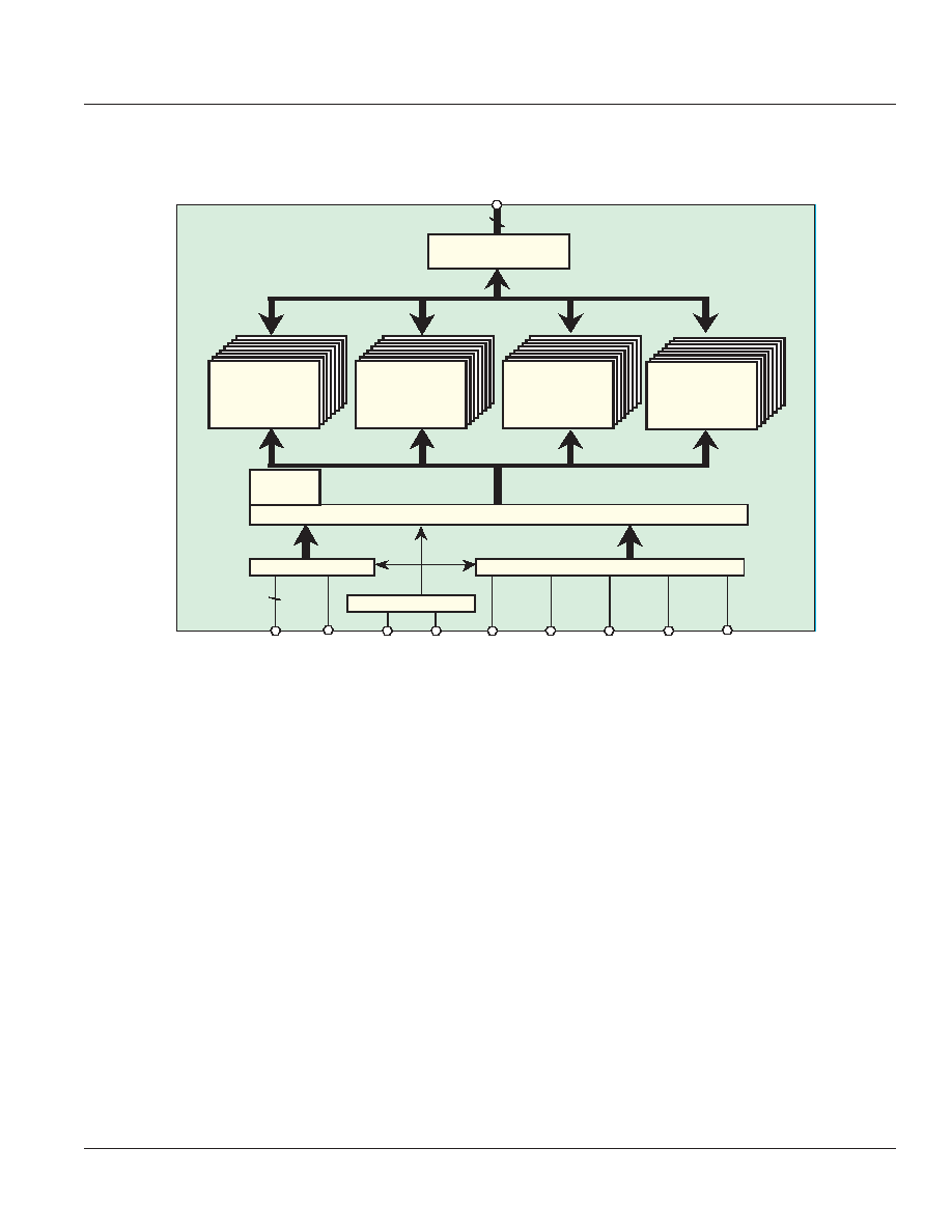
BLOCK DIAGRAM
DQ0-7
Address Buffer
Control Signal Buffer
Clock Buffer
Control Circuitry
I/O Buffer
Mode
Register
Memory Array
Bank #0
8192x1024x8
Cell Array
Memory Array
Bank #1
Cell Array
Memory Array
Bank #2
Cell Array
Memory Array
Bank #3
Cell Array
8192x1024x8
8192x1024x8
8192x1024x8
A0-12
BA0,1
CLK
CKE
/CS
/RAS
/CAS
/WE
DQM
Note:This figure shows the IS42S83200A
The IS42S16160A configuration is 8192x512x16 of cell array and DQ0-15

4
Integrated Silicon Solution, Inc. -- 1-800-379-4774
Rev. D
11/01/05
ISSI
Æ
IS42S83200A
(4-bank x 8,388,608 - word x 8-bit)
IS42S16160A
(4-bank x 4,194,304 - word x 16-bit)
PIN FUNCTION
CLK
Input
Master Clock:
All other inputs are referenced to the rising edge of CLK
CKE
Input
Clock Enable:
CKE controls internal clock.When CKE is low, internal clock for
the following cycle is ceased. CKE is also used to select
auto / self-refresh.
After self-refresh mode is started, CKE becomes asynchronous input.
Self-refresh is maintained as long as CKE is low.
/CS
Input
Chip Select:
When /CS is high, any command means No Operation.
/RAS, /CAS, /WE
Input
Combination of /RAS, /CAS, /WE defines basic commands.
A0-12
Input
A0-12 specify the Row / Column Address in conjunction with BA0,1.
The Row Address is specified by A0-12.
The Column Address is specified by A0-9(x8)/A0-8(x16).
A10 is also used to indicate precharge option. When A10 is high at a
read / write command, an auto precharge is performed. When A10 is
high at a precharge command, all banks are precharged.
BA0,1
Input
Bank Address:
BA0,1 specifies one of four banks to which a command is applied.
BA0,1 must be set with ACT, PRE , READ , WRITE commands.
DQ0-7(x8),
DQ0-15(x16)
Input / Output
Data In and Data out are referenced to the rising edge of CLK.
DQM(x8),
DQMU/L(x16)
Input
Din Mask / Output Disable:
When DQM(U/L) is high in burst write, Din for the current cycle is
masked. When DQM(U/L) is high in burst read,
Dout is disabled at the next but one cycle.
Vdd, Vss
Power Supply
Power Supply for the memory array and peripheral circuitry.
VddQ, VssQ
Power Supply
VddQ and VssQ are supplied to the Output Buffers only.

Integrated Silicon Solution, Inc. -- 1-800-379-4774
5
Rev. D
11/01/05
ISSI
Æ
IS42S83200A
(4-bank x 8,388,608 - word x 8-bit)
IS42S16160A
(4-bank x 4,194,304 - word x 16-bit)
BASIC FUNCTIONS
The IS42S83200A/16160A provides basic
functions, bank (row) activate, burst read / write, bank (row)
precharge, and auto / self refresh.
Each command is defined by control signals of /RAS,
CLK
/CAS and /WE at CLK rising edge. In addition to 3 signals,
/CS, CKE and A10 are used as chip select, refresh opt ion,
and precharge option, respectively .
To know the detailed definition of commands,
please see the command truth table.
/CS
Chip Select : L=select, H=deselect
/RAS
Command
/CAS
Command
define basic command
/WE
Command
CKE
Refresh Option @ refresh command
A10
Precharge Option @ precharge or read/write command
Activate (ACT) [/RAS =L, /CAS =/WE =H]
ACT command activates a row in an idle bank indicated by BA.
Read (READ) [/RAS =H, /CAS =L, /WE =H]
READ command starts burst read from the active bank indicated by BA.
First output data appears after /CAS latency. When A10 =H at this command,
the bank is deactivated after the burst read (auto-precharge, READA).
Write (WRITE) [/RAS =H, /CAS =/WE =L]
WRITE command starts burst write to the active bank indicated by BA. Total
data length to be written is set by burst length. When A10 =H at this command,
the bank is deactivated after the burst write (auto-precharge, WRITEA).
Precharge (PRE) [/RAS =L, /CAS =H, /WE =L]
PRE command deactivates the active bank indicated by BA. This com
mand also terminates burst read / write operation. When A10 =H at this
command, all banks are deactivated (precharge all, PREA ).
Auto-Refresh (REFA) [/RAS =/CAS =L, /WE =CKE =H]
REFA command starts auto-refresh cycle. Refresh address including bank
address are generated internally. After this command, the banks are
precharged automatically.

6
Integrated Silicon Solution, Inc. -- 1-800-379-4774
Rev. D
11/01/05
ISSI
Æ
IS42S83200A
(4-bank x 8,388,608 - word x 8-bit)
IS42S16160A
(4-bank x 4,194,304 - word x 16-bit)
COMMAND TRUTH TABLE
COMMAND
MNEMONIC CKE
n-1
CKE
n
/CS
/RAS /CAS
/WE BA0,1
A10
/AP
A0-9,
11-12
note
Deselect
DESEL
H
X
H
X
X
X
X
X
X
No Operation
NOP
H
X
L
H
H
H
X
X
X
Row Address Entry &
Bank Activate
ACT
H
X
L
L
H
H
V
V
V
Single Bank Precharge
PRE
H
X
L
L
H
L
V
L
X
Precharge All Banks
PREA
H
X
L
L
H
L
X
H
X
Column Address Entry
& Write
WRITE
H
X
L
H
L
L
V
L
V
Column Address Entry
& Write with
Auto-Precharge
WRITEA
H
X
L
H
L
L
V
H
V
Column Address Entry
& Read
READ
H
X
L
H
L
H
V
L
V
Column Address Entry
& Read with
Auto-Precharge
READA
H
X
L
H
L
H
V
H
V
Auto-Refresh
REFA
H
H
L
L
L
H
X
X
X
Self-Refresh Entry
REFS
H
L
L
L
L
H
X
X
X
Self-Refresh Exit
REFSX
L
H
H
X
X
X
X
X
X
L
H
L
H
H
H
X
X
X
Burst Terminate
TBST
H
X
L
H
H
L
X
X
X
Mode Register Set
MRS
H
X
L
L
L
L
L
L
V
1
H=High Level, L=Low Level, V=Valid, X=Don't Care, n=CLK cycle number
NOTE:
1. A7-9,11-12=L, A0-A6 =Mode Address

Integrated Silicon Solution, Inc. -- 1-800-379-4774
7
Rev. D
11/01/05
ISSI
Æ
IS42S83200A
(4-bank x 8,388,608 - word x 8-bit)
IS42S16160A
(4-bank x 4,194,304 - word x 16-bit)
FUNCTION TRUTH TABLE
Current State
/CS
/RAS /CAS /WE
Address
Command
Action
IDLE
H
X
X
X
X
DESEL
NOP
L
H
H
H
X
NOP
NOP
L
H
H
L
X
TBST
ILLEGAL*2
L
H
L
X
BA, CA, A10
READ / WRITE ILLEGAL*2
L
L
H
H
BA, RA
ACT
Bank Active, Latch RA
L
L
H
L
BA, A10
PRE / PREA
NOP*4
L
L
L
H
X
REFA
Auto-Refresh*5
L
L
L
L
Op-Code,
Mode-Add
MRS
Mode Register Set*5
ROW
ACTIVE
H
X
X
X
X
DESEL
NOP
L
H
H
H
X
NOP
NOP
L
H
H
L
X
TBST
NOP
L
H
L
H
BA, CA, A10
READ / READA
Begin Read, Latch CA,
Determine Auto-Precharge
L
H
L
L
BA, CA, A10
WRITE /
WRITEA
Begin Write, Latch CA,
Determine Auto-Precharge
L
L
H
H
BA, RA
ACT
Bank Active / ILLEGAL*2
L
L
H
L
BA, A10
PRE / PREA
Precharge / Precharge All
L
L
L
H
X
REFA
ILLEGAL
L
L
L
L
Op-Code,
Mode-Add
MRS
ILLEGAL
READ
H
X
X
X
X
DESEL
NOP (Continue Burst to END)
L
H
H
H
X
NOP
NOP (Continue Burst to END)
L
H
H
L
X
TBST
Terminate Burst
L
H
L
H
BA, CA, A10
READ / READA
Terminate Burst, Latch CA,
Begin New Read, Determine
Auto-Precharge*3
L
H
L
L
BA, CA, A10
WRITE /
WRITEA
Terminate Burst, Latch CA,
Begin Write, Determine Auto-
Precharge*3
L
L
H
H
BA, RA
ACT
Bank Active / ILLEGAL*2
L
L
H
L
BA, A10
PRE / PREA
Terminate Burst, Precharge
L
L
L
H
X
REFA
ILLEGAL
L
L
L
L
Op-Code,
Mode-Add
MRS
ILLEGAL

8
Integrated Silicon Solution, Inc. -- 1-800-379-4774
Rev. D
11/01/05
ISSI
Æ
IS42S83200A
(4-bank x 8,388,608 - word x 8-bit)
IS42S16160A
(4-bank x 4,194,304 - word x 16-bit)
FUNCTION TRUTH TABLE (continued)
Current State
/CS
/RAS /CAS /WE
Address
Command
Action
WRITE
H
X
X
X
X
DESEL
NOP (Continue Burst to END)
L
H
H
H
X
NOP
NOP (Continue Burst to END)
L
H
H
L
X
TBST
Terminate Burst
L
H
L
H
BA, CA, A10
READ / READA
Terminate Burst, Latch CA,
Begin Read, Determine Auto-
Precharge*3
L
H
L
L
BA, CA, A10
WRITE /
WRITEA
Terminate Burst, Latch CA,
Begin Write, Determine Auto-
Precharge*3
L
L
H
H
BA, RA
ACT
Bank Active / ILLEGAL*2
L
L
H
L
BA, A10
PRE / PREA
Terminate Burst, Precharge
L
L
L
H
X
REFA
ILLEGAL
L
L
L
L
Op-Code,
Mode-Add
MRS
ILLEGAL
READ with
AUTO
PRECHARGE
H
X
X
X
X
DESEL
NOP (Continue Burst to END)
L
H
H
H
X
NOP
NOP (Continue Burst to END)
L
H
H
L
X
TBST
ILLEGAL
L
H
L
H
BA, CA, A10
READ / READA ILLEGAL
L
H
L
L
BA, CA, A10
WRITE /
WRITEA
ILLEGAL
L
L
H
H
BA, RA
ACT
Bank Active / ILLEGAL*2
L
L
H
L
BA, A10
PRE / PREA
ILLEGAL*2
L
L
L
H
X
REFA
ILLEGAL
L
L
L
L
Op-Code,
Mode-Add
MRS
ILLEGAL
WRITE with
AUTO
PRECHARGE
H
X
X
X
X
DESEL
NOP (Continue Burst to END)
L
H
H
H
X
NOP
NOP (Continue Burst to END)
L
H
H
L
X
TBST
ILLEGAL
L
H
L
H
BA, CA, A10
READ / READA ILLEGAL
L
H
L
L
BA, CA, A10
WRITE /
WRITEA
ILLEGAL
L
L
H
H
BA, RA
ACT
Bank Active / ILLEGAL*2
L
L
H
L
BA, A10
PRE / PREA
ILLEGAL*2
L
L
L
H
X
REFA
ILLEGAL
L
L
L
L
Op-Code,
Mode-Add
MRS
ILLEGAL

Integrated Silicon Solution, Inc. -- 1-800-379-4774
9
Rev. D
11/01/05
ISSI
Æ
IS42S83200A
(4-bank x 8,388,608 - word x 8-bit)
IS42S16160A
(4-bank x 4,194,304 - word x 16-bit)
FUNCTION TRUTH TABLE (continued)
Current State
/CS
/RAS /CAS /WE
Address
Command
Action
PRE -
CHARGING
H
X
X
X
X
DESEL
NOP (Idle after tRP)
L
H
H
H
X
NOP
NOP (Idle after tRP)
L
H
H
L
X
TBST
ILLEGAL*2
L
H
L
X
BA, CA, A10
READ / WRITE ILLEGAL*2
L
L
H
H
BA, RA
ACT
ILLEGAL*2
L
L
H
L
BA, A10
PRE / PREA
NOP*4 (Idle after tRP)
L
L
L
H
X
REFA
ILLEGAL
L
L
L
L
Op-Code,
Mode-Add
MRS
ILLEGAL
ROW
ACTIVATING
H
X
X
X
X
DESEL
NOP (Row Active after tRCD)
L
H
H
H
X
NOP
NOP (Row Active after tRCD)
L
H
H
L
X
TBST
ILLEGAL*2
L
H
L
X
BA, CA, A10
READ / WRITE ILLEGAL*2
L
L
H
H
BA, RA
ACT
ILLEGAL*2
L
L
H
L
BA, A10
PRE / PREA
ILLEGAL*2
L
L
L
H
X
REFA
ILLEGAL
L
L
L
L
Op-Code,
Mode-Add
MRS
ILLEGAL
WRITE RE-
COVERING
H
X
X
X
X
DESEL
NOP
L
H
H
H
X
NOP
NOP
L
H
H
L
X
TBST
ILLEGAL*2
L
H
L
X
BA, CA, A10
READ / WRITE ILLEGAL*2
L
L
H
H
BA, RA
ACT
ILLEGAL*2
L
L
H
L
BA, A10
PRE / PREA
ILLEGAL*2
L
L
L
H
X
REFA
ILLEGAL
L
L
L
L
Op-Code,
Mode-Add
MRS
ILLEGAL

10
Integrated Silicon Solution, Inc. -- 1-800-379-4774
Rev. D
11/01/05
ISSI
Æ
IS42S83200A
(4-bank x 8,388,608 - word x 8-bit)
IS42S16160A
(4-bank x 4,194,304 - word x 16-bit)
FUNCTION TRUTH TABLE (continued)
Current State
/CS
/RAS /CAS /WE
Address
Command
Action
RE-
FRESHING
H
X
X
X
X
DESEL
NOP (Idle after tRC)
L
H
H
H
X
NOP
NOP (Idle after tRC)
L
H
H
L
X
TBST
ILLEGAL
L
H
L
X
BA, CA, A10
READ / WRITE ILLEGAL
L
L
H
H
BA, RA
ACT
ILLEGAL
L
L
H
L
BA, A10
PRE / PREA
ILLEGAL
L
L
L
H
X
REFA
ILLEGAL
L
L
L
L
Op-Code,
Mode-Add
MRS
ILLEGAL
MODE
REGISTER
SETTING
H
X
X
X
X
DESEL
NOP (Idle after tRSC)
L
H
H
H
X
NOP
NOP (Idle after tRSC)
L
H
H
L
X
TBST
ILLEGAL
L
H
L
X
BA, CA, A10
READ / WRITE ILLEGAL
L
L
H
H
BA, RA
ACT
ILLEGAL
L
L
H
L
BA, A10
PRE / PREA
ILLEGAL
L
L
L
H
X
REFA
ILLEGAL
L
L
L
L
Op-Code,
Mode-Add
MRS
ILLEGAL
ABBREVIATIONS:
H=High Level, L=Low Level, X=Don't Care
BA=Bank Address, RA=Row Address, CA=Column Address, NOP=No OPeration
NOTES:
1. All entries assume that CKE was High during the preceding clock cycle and the current clock cycle.
2. ILLEGAL to bank in specified state; function may be legal in the bank indicated by BA, depending on the state of
that bank.
3. Must satisfy bus contention, bus turn around, write recovery requirements.
4. NOP to bank precharging or in idle state. May precharge bank indicated by BA.
5. ILLEGAL if any bank is not idle.
ILLEGAL = Device operation and/or data-integrity are not guaranteed.
Integrated Silicon Solution, Inc. -- 1-800-379-4774
11
Rev. D
11/01/05
ISSI
Æ
IS42S83200A
(4-bank x 8,388,608 - word x 8-bit)
IS42S16160A
(4-bank x 4,194,304 - word x 16-bit)
FUNCTION TRUTH TABLE (continued)
Current State
CKE
n-1
CKE
n
/CS /RAS /CAS /WE Add
Action
SELF-
REFRESH*1
H
X
X
X
X
X
X
INVALID
L
H
H
X
X
X
X
Exit Self-Refresh (Idle after tRC)
L
H
L
H
H
H
X
Exit Self-Refresh (Idle after tRC)
L
H
L
H
H
L
X
ILLEGAL
L
H
L
H
L
X
X
ILLEGAL
L
H
L
L
X
X
X
ILLEGAL
L
L
X
X
X
X
X
NOP (Maintain Self-Refresh)
POWER
DOWN
H
X
X
X
X
X
X
INVALID
L
H
X
X
X
X
X
Exit Power Down to Idle
L
L
X
X
X
X
X
NOP (Maintain Power Down)
ALL BANKS
IDLE*2
H
H
X
X
X
X
X
Refer to Function Truth Table
H
L
L
L
L
H
X
Enter Self-Refresh
H
L
H
X
X
X
X
Enter Power Down
H
L
L
H
H
H
X
Enter Power Down
H
L
L
H
H
L
X
ILLEGAL
H
L
L
H
L
X
X
ILLEGAL
H
L
L
L
X
X
X
ILLEGAL
L
X
X
X
X
X
X
Refer to Current State =Power Down
ANY STATE
other than
listed above
H
H
X
X
X
X
X
Refer to Function Truth Table
H
L
X
X
X
X
X
Begin CLK Suspend at Next Cycle*3
L
H
X
X
X
X
X
Exit CLK Suspend at Next Cycle*3
L
L
X
X
X
X
X
Maintain CLK Suspend
ABBREVIATIONS:
H=High Level, L=Low Level, X=Don't Care
NOTES:
1. CKE Low to High transition will re-enable CLK and other inputs
asynchronously
. A minimum setup time must be
satisfied before any command other than EXIT.
2. Self-Refresh can be entered only from the All Banks Idle State.
3. Must be legal command.
12
Integrated Silicon Solution, Inc. -- 1-800-379-4774
Rev. D
11/01/05
ISSI
Æ
IS42S83200A
(4-bank x 8,388,608 - word x 8-bit)
IS42S16160A
(4-bank x 4,194,304 - word x 16-bit)
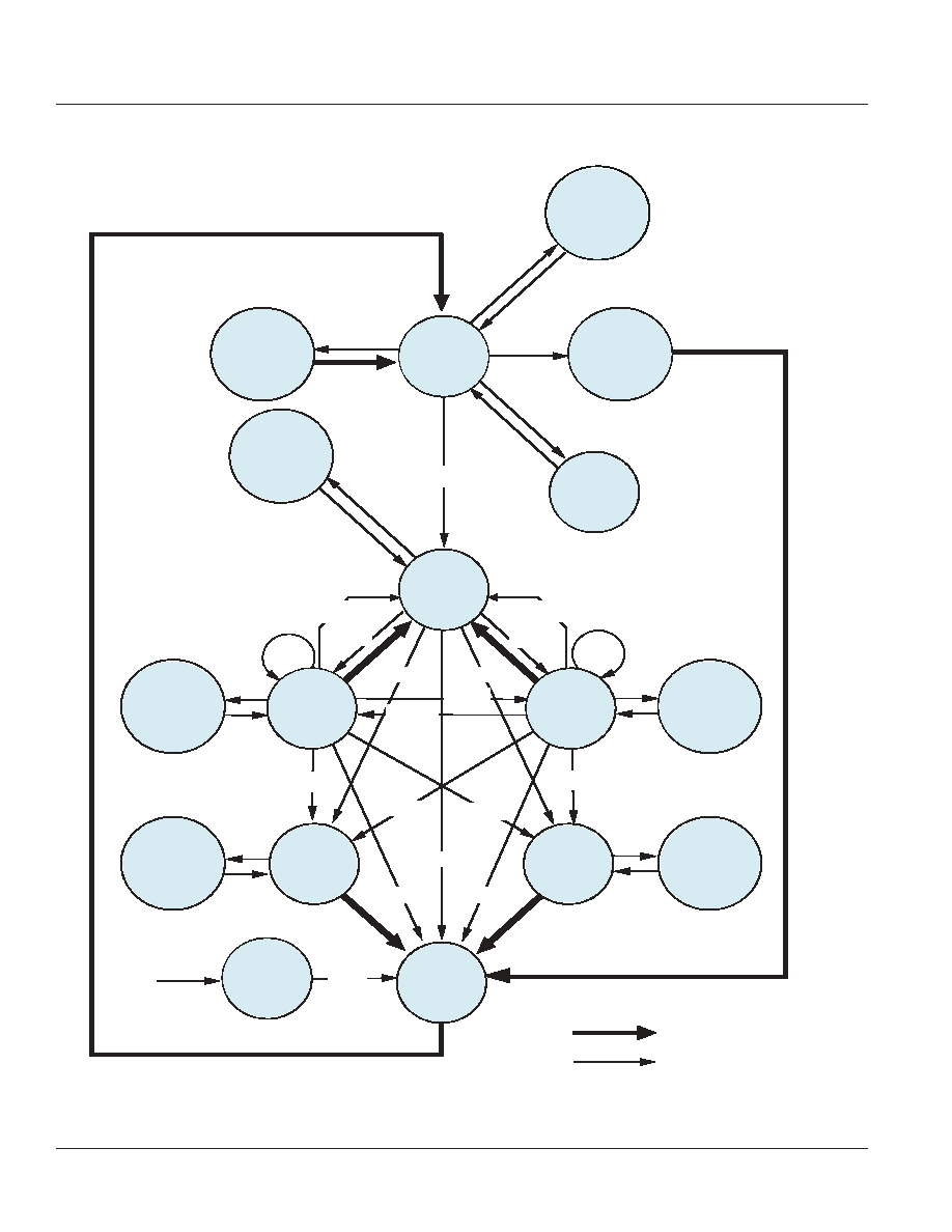
SIMPLIFIED STATE DIAGRAM
REFS
SELF
REFRESH
CKEL
CKEH
CKEL
CKEH
CKEL
CKEH
CKEL
CKEH
ACT
REFA
REFSX
CKEL
CKEH
MRS
CKEL
CKEH
WRITE
READ
WRITEA
WRITEA
READA
WRITE
READ
PRE
READA
WRITEA
READA
PRE
PRE
PRE
POWER
APPLIED
Automatic Sequence
Command Sequence
CLK
SUSPEND
MODE
REGISTER
SET
IDLE
AUTO
REFRESH
WRITE
SUSPEND
WRITE
WRITEA
SUSPEND
WRITEA
POWER
ON
PRE
CHARGE
READA
READ
READ
SUSPEND
ROW
ACTIVE
POWER
DOWN
READA
SUSPEND
TERM
TERM

Integrated Silicon Solution, Inc. -- 1-800-379-4774
13
Rev. D
11/01/05
ISSI
Æ
IS42S83200A
(4-bank x 8,388,608 - word x 8-bit)
IS42S16160A
(4-bank x 4,194,304 - word x 16-bit)
POWER ON SEQUENCE
Before starting normal operation, the following
power on sequence is necessary to prevent a
SDRAM from damaged or malfunctioning.
1. Apply power and start clock. Attempt to maintain
CKE high, DQM high and NOP condition at the
inputs.
2. Maintain stable power, stable clock, and NOP
input conditions for a minimum of 200µs.
3. Issue precharge commands for all banks. (PRE
or PREA)
4. After all banks become idle state (after tRP),
issue 8 or more auto-refresh commands.
5. Issue a mode register set command to initialize
the mode register.
After these sequence, the SDRAM is idle state and
ready for normal operation.
MODE REGISTER
Burst Length, Burst Type and /CAS Latency can
be programmed by setting the mode register
(MRS). The mode register stores these data until
the next MRS command, which may be issued
when all banks are in idle state. After tRSC from a
MRS command, the SDRAM is ready for new
command.
CLK
/CS
/RAS
/CAS
/WE
BA0,1 A12-A0
V
BA0 BA1 A12 A11 A10 A9 A8 A7 A6 A5 A4 A3 A2 A1 A0
0
0
0
0
0 SW
0
0
LTMODE
BT
BL
BURST
LENGTH
BL
BT=0
BT=1
0 0 0
0 0 1
0 1 0
0 1 1
1 0 0
1 0 1
1 1 0
1 1 1
1
2
4
8
R
R
R
Full Page
1
2
4
8
R
R
R
R
0
1
BURST
TYPE
SEQUENTIAL
INTERLEAVED
LATENCY
MODE
CL
/CAS LATENCY
0 0 0
0 0 1
0 1 0
0 1 1
1 0 0
1 0 1
1 1 0
1 1 1
R
R
2
3
R
R
R
R
Burst Write
Single Write
SW
0
1
R: Reserved for Future Use

14
Integrated Silicon Solution, Inc. -- 1-800-379-4774
Rev. D
11/01/05
ISSI
Æ
IS42S83200A
(4-bank x 8,388,608 - word x 8-bit)
IS42S16160A
(4-bank x 4,194,304 - word x 16-bit)
CLK
Command
Address
DQ
Read
Y
Write
Y
/CAS Latency
Burst Length
Burst Length
CL= 3
BL= 4
Q0
Q1
Q2
Q3
D0
D1
D2
D3
Burst Type
A2 A1 A0
Initial Address BL
Sequential
Interleaved
Column Addressing
0
0
0
1
0
0
0
1
1
0
1
1
1
0
1
1
-
0
-
1
-
0
-
1
-
0
0
2
5
1
4
1
3
6
0
5
2
4
7
3
6
3
5
0
2
7
4
6
1
5
0
5
7
2
4
1
6
0
3
7
2
7
1
0
2
1
3
2
0
3
0
7
6
0
1
1
0
2
3
3
0
-
1
1
1
3
4
3
1
1
8
4
2
0
0
1
1
0
0
1
1
0
0
1
1
-
1
4
3
0
7
6
3
2
7
6
5
2
5
4
1
0
7
2
3
6
7
4
3
6
5
2
1
0
1
0
5
4
7
4
7
6
3
2
1
0
1
4
5
6
5
0
7
4
3
2
7
6
3
2
1
6
1
0
5
4
3
6
7
2
3
0
7
2
1
6
5
4
5
4
1
0
3
0
2
1
3
2
0
3
1
0
1
4
5
3
2
2
3
1
0
2
1
-
2
0
6
5
0
1
2
0
0

Integrated Silicon Solution, Inc. -- 1-800-379-4774
15
Rev. D
11/01/05
ISSI
Æ
IS42S83200A
(4-bank x 8,388,608 - word x 8-bit)
IS42S16160A
(4-bank x 4,194,304 - word x 16-bit)
OPERATIONAL DESCRIPTION
BANK ACTIVATE
The SDRAM has four independent banks. Each bank
is activated by the ACT command with the bank ad-
dresses (BA0,1). A row is indicated by the row ad-
dresses A0-12. The minimum activation interval be-
tween one bank and the other bank is tRRD.Multiple
banks can be active state concurrently by issuing mul
tiple ACT commands.
PRECHARGE
The PRE command deactivates the bank indicated
by BA0,1. When multiple banks are active, the
precharge all command (PREA, PRE + A10=H) is
available to deactivate them at the same time.
After tRP from the precharge, an ACT command to the
same bank can be issued.BA0-1 are
"DON'T CARE"
in this case.
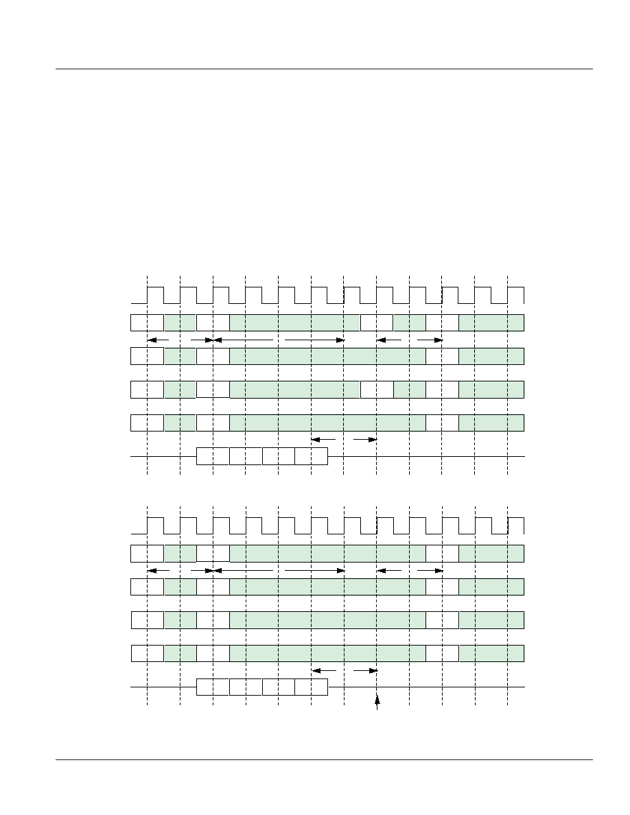
READ
After tRCD from the bank activation, a READ
command can be issued. 1st output data is avail-
able after the /CAS Latency from the READ, fol
lowed by (BL -1) consecutive data when the Burst
Length is BL. The start address is specified by
A0-9(X8), A0-8(X16) , and the address sequence of
burst data is defined by the Burst Type.
A READ command may be applied to any
active bank, so the row precharge time (tRP) can be
hidden behind continuous output data by
interleaving the multiple banks. When A10 is high
at a READ command, the auto-precharge
(READA) is performed. Any command (READ,
WRITE, PRE, TBST, ACT) to the same bank is
inhibited till the internal precharge is complete.
The internal precharge starts at BL after READA.
The next ACT command can be issued after (BL
+ tRP) from the previous READA.
In any case, tRCD+BL
tRASmin must be met.
Bank Activation and Precharge All (BL=4, CL=3)
CLK
Command
A0-9,11-12
A10
BA0-1
DQ
ACT
READ
ACT
PRE
ACT
Xa
Xb
Yb
Xa
1
Xa
Xb
0
00
01
01
00
Qb0
Qb1
Qb2
Qb3
tRRD
tRCD
tRP
Xa
Precharge All

16
Integrated Silicon Solution, Inc. -- 1-800-379-4774
Rev. D
11/01/05
ISSI
Æ
IS42S83200A
(4-bank x 8,388,608 - word x 8-bit)
IS42S16160A
(4-bank x 4,194,304 - word x 16-bit)
ACT
READ
ACT
PRE
ACT
Xa
Xb
Yb
Xa
0
Xa
Xb
0
00
01
01
00
Qb0
Qb1
Qb2
Qb3
tRCD
tRCD
tRP
Xa
Multi Bank Interleaving Read (CL=2, BL=4)
READ
Ya
0
00
Qa0
Qa1
Qa2
Qa3
00
CLK
Command
A0-9,11-12
A10
BA0-1
DQ
Read with Auto-Precharge (CL=2, BL=4)
CLK
Command
A0-9,11-12
A10
BA0-1
DQ
internal precharge starts
Auto-Precharge Timing (READ, BL=4)
CLK
Command
DQ
ACT
ACT
Xa
Xa
Xa
00
00
tRCD
tRP
Xa
READ
Ya
1
00
Qa0
Qa1
Qa2
Qa3
BL
ACT
ACT
tRCD
READ
Qa0
Qa1
Qa2
Qa3
BL
Qa0
Qa1
Qa2
Qa3
CL=2
CL=3
DQ
internal precharge starts
Integrated Silicon Solution, Inc. -- 1-800-379-4774
17
Rev. D
11/01/05
ISSI
Æ
IS42S83200A
(4-bank x 8,388,608 - word x 8-bit)
IS42S16160A
(4-bank x 4,194,304 - word x 16-bit)
WRITE
A WRITE command can be issued to any active bank.
The start address is specified by A0-9(x8), A0-8(x16).
1st input data is set at the same cycle as the WRITE.
The consecutive data length to be write is defined
by the Burst Length. The address sequence of
burst data is defined by Burst Type. Minmum delay
time of a WRITE command after an ACT command to
the same bank is tRCD. From the last input data to the
PRE command , the write recovery time (tWR) is
required. When A10 is high at a WRITE command ,
auto-precharge (WRITEA) is performed. Any com
mand (READ,WRITE,PRE,ACT,TBST) to the same
bank is inhibited till the internal precharge is complete.
The internal precharge starts at tWR after the last input
data cycle . The next ACT command can be issued
after (BL+tWR-1+tRP) from the previous WRITEA. In
any case, tRCD+BL+tWR-1
tRASmin must be met.
Write (BL=4)
CLK
Command
A0-9,11-12
A10
BA0-1
DQ
Write with Auto-Precharge (BL=4)
CLK
Command
A0-9,11-12
A10
BA0-1
DQ
ACT
PRE
ACT
Xa
Xa
0
Xa
00
00
tRCD
tRP
Xa
Write
Ya
0
00
Da0
Da1
Da2
Da3
BL
tWR
ACT
ACT
Xa
Xa
Xa
00
00
tRCD
tRP
Xa
Write
Ya
1
00
Da0
Da1
Da2
Da3
BL
tWR
internal precharge starts

18
Integrated Silicon Solution, Inc. -- 1-800-379-4774
Rev. D
11/01/05
ISSI
Æ
IS42S83200A
(4-bank x 8,388,608 - word x 8-bit)
IS42S16160A
(4-bank x 4,194,304 - word x 16-bit)
BURST INTERRUPTION
[ Read Interrupted by Read ]
Burst read operation can be interrupted by new read of any bank. Random column access is allowed
READ to READ interval is minimum 1 CLK..
Read interrupted by Read (CL=2, BL=4)
CLK
Command
A0-9,11-12
A10
BA0-1
DQ
READ
Yb
0
00
Qc0
Qc1
Qc2
Qc3
READ
Ya
0
00
Qa0
Qa1
Qa2
Qb0
READ
Yc
0
10
[ Read Interrupted by Write ]
Burst read operation can be interrupted by write of any bank. Random column access is allowed. In this case, the
DQ should be controlled adequately by using the DQM to prevent the bus contention. The output is disabled
automatically 2 cycle after WRITE assertion.
Read interrupted by Write (CL=2, BL=4)
CLK
Command
A0-9,11-12
A10
BA0-1
DQM
DQ
ACT
Xa
Xa
00
READ
Ya
0
00
Qa0
Da0
Da1
Da2
Write
Ya
0
00
Da3
Output disable by DQM
by WRITE
Integrated Silicon Solution, Inc. -- 1-800-379-4774
19
Rev. D
11/01/05
ISSI
Æ
IS42S83200A
(4-bank x 8,388,608 - word x 8-bit)
IS42S16160A
(4-bank x 4,194,304 - word x 16-bit)
[ Read Interrupted by Precharge ]
Burst read operation can be interrupted by precharge
of the same bank . READ to PRE interval is minimum 1
CLK. A PRE command to output disable latency is
equivalent to the /CAS Latency. As a result, READ to
PRE interval determines valid data length to be output.
The figure below shows examples of BL=4.
Read interrupted by Precharge (BL=4)
CLK
Command
PRE
READ
Q0
Q1
Q2
PRE
READ
Q0
Q1
PRE
READ
Q0
PRE
READ
Q0
Q1
Q2
PRE
READ
Q0
Q1
PRE
READ
Q0
CL=2
CL=3
DQ
Command
DQ
Command
DQ
Command
DQ
Command
DQ
Command
DQ

20
Integrated Silicon Solution, Inc. -- 1-800-379-4774
Rev. D
11/01/05
ISSI
Æ
IS42S83200A
(4-bank x 8,388,608 - word x 8-bit)
IS42S16160A
(4-bank x 4,194,304 - word x 16-bit)
[Read Interrupted by Burst Terminate]
Similarly to the precharge, a burst terminate command
can interrupt the burst read operation and disable the
data output. The terminated bank remains active.
READ to TBST interval is minimum 1 CLK. A TBST
command to output disable latency is equivalent to
the /CAS Latency.
Read interrupted by Terminate (BL=4)
CL=2
CL=3
CLK
Command
DQ
Command
DQ
Command
DQ
Command
DQ
Command
DQ
Command
DQ
TBST
READ
Q0
Q1
Q2
TBST
READ
Q0
Q1
TBST
READ
Q0
TBST
READ
Q0
Q1
Q2
TBST
READ
Q0
Q1
TBST
READ
Q0

Integrated Silicon Solution, Inc. -- 1-800-379-4774
21
Rev. D
11/01/05
ISSI
Æ
IS42S83200A
(4-bank x 8,388,608 - word x 8-bit)
IS42S16160A
(4-bank x 4,194,304 - word x 16-bit)
[ Write Interrupted by Write ]
Burst write operation can be interrupted by new write of any bank. Random column access is allowed. WRITE to
WRITE interval is minimum 1 CLK.
Write interrupted by Write (BL=4)
CLK
Command
A0-9,11-12
A10
BA0-1
DQ
Write
Yb
0
00
Dc0
Dc1
Dc2
Dc3
Write
Ya
0
00
Da0
Da1
Da2
Db0
Write
Yc
0
10
[ Write Interrupted by Read ]
Burst write operation can be interrupted by read of the same or the other bank. Random column access is
allowed. WRITE to READ interval is minimum 1 CLK. The input data on DQ at the interrupting READ cycle is
"don't care".
Write interrupted by Read (CL=2, BL=4)
CLK
Command
A0-9,11-12
A10
BA0-1
DQ
ACT
Xa
Xa
00
READ
Yb
0
00
Da0
Da1
Qb0
Write
Ya
0
00
Qb1
Qb2
Qb3
don't care

22
Integrated Silicon Solution, Inc. -- 1-800-379-4774
Rev. D
11/01/05
ISSI
Æ
IS42S83200A
(4-bank x 8,388,608 - word x 8-bit)
IS42S16160A
(4-bank x 4,194,304 - word x 16-bit)
[ Write Interrupted by Precharge ]
Burst write operation can be interrupted by precharge of the same bank.Write recovery time(tWR) is
required from the last data to PRE command. During write recovery, data inputs must be masked by DQM.
Write interrupted by Precharge (BL=4)
CLK
Command
A0-9,11-12
A10
BA0-1
DQM
DQ
Write
Ya
0
00
ACT
Xa
0
00
Da0
Da1
PRE
0
00
ACT
Xa
0
00
tWR
tRP
[Write Interrupted by Burst Terminate]
Burst terminate command can terminate burst write operation.In this case, the write recovery time is not
required and the bank remains active. WRITE to TBST interval is minimum 1 CLK.
Write interrupted by Terminate (BL=4)
CLK
Command
A0-9,11-12
A10
BA0-1
DQ
Write
Ya
0
00
ACT
Xa
0
00
Da0
Da1
TBST
Write
Yb
0
00
Db0
Db1
Db2
Db3

Integrated Silicon Solution, Inc. -- 1-800-379-4774
23
Rev. D
11/01/05
ISSI
Æ
IS42S83200A
(4-bank x 8,388,608 - word x 8-bit)
IS42S16160A
(4-bank x 4,194,304 - word x 16-bit)
[Write with Auto-Precharge Interrupted by Write or Read to another Bank]
Burst write with auto-precharge can be interrupted by write or read to another bank. Next ACT command
can be issued after(BL+tWR-1+ tRP) from the WRITEA. Auto-precharge interruption by a command to the
same bank is inhibited.
WRITEA interrupted by WRITE to another bank (BL=4)
CLK
Command
A0-9,11-12
A10
BA0-1
DQ
Db0
Db1
Db2
Db3
Write
Ya
1
00
Da0
Da1
Write
Yb
0
10
BL
tWR
tRP
ACT
Xa
Xa
00
auto-precharge interrupted
activate
WRITEA interrupted by READ to another bank (CL=2, BL=4)
CLK
Command
A0-9,11-12
A10
BA0-1
DQ
Write
Ya
1
00
Da0
Da1
Read
Yb
0
10
BL
tWR
tRP
ACT
Xa
Xa
00
Qb0
Qb1
Qb2
Qb3
auto-precharge interrupted
activate

24
Integrated Silicon Solution, Inc. -- 1-800-379-4774
Rev. D
11/01/05
ISSI
Æ
IS42S83200A
(4-bank x 8,388,608 - word x 8-bit)
IS42S16160A
(4-bank x 4,194,304 - word x 16-bit)
[Read with Auto-Precharge Interrupted by Read to another Bank]
Burst write with auto-precharge can be interrupted by write or read to another bank. Next ACT command
can be issued after (BL+tRP) from the READA. Auto-precharge interruption by a command to the same
bank is inhibited.
READA interrupted by READ to another bank (CL=2, BL=4)
CLK
Command
Read
Ya
1
00
Qa0
Qa1
Read
Yb
0
10
BL
tRP
ACT
Xa
Xa
00
Qb0
Qb1
Qb2
Qb3
A0-9,11-12
A10
BA0-1
DQ
auto-precharge interrupted
activate
[Full Page Burst]
Full page burst length is available for only the sequential burst type. Full page burst read or write is
repeated untill a Precharge or a Burst Terminate command is issued. In case of the full page burst, a read
or write with auto-precharge command is illegal.
[Single Write]
When single write mode is set, burst length for write is always one, independently of Burst Length defined
by (A2-0).

Integrated Silicon Solution, Inc. -- 1-800-379-4774
25
Rev. D
11/01/05
ISSI
Æ
IS42S83200A
(4-bank x 8,388,608 - word x 8-bit)
IS42S16160A
(4-bank x 4,194,304 - word x 16-bit)
AUTO REFRESH
Single cycle of auto-refresh is initiated with a REFA
(/CS= /RAS= /CAS= L, /WE= /CKE= H) command.
The refresh address is generated internally. 8192
REFA cycles within 64ms refresh 256M bit memory
cells. The auto-refresh is performed on 4 banks
concurrently. Before performing an auto-refresh, all
banks must be in the idle state. Auto-refresh to auto-
refresh interval is minimum tRFC. Any command must
not be supplied to the device before tRFC from the
REFA command.
Auto-Refresh
CLK
/CS
/RAS
/CAS
/WE
NOP or DESELECT
minimum tRFC
CKE
A0-12
BA0-1
Auto Refresh on All Banks
Auto Refresh on All Banks

26
Integrated Silicon Solution, Inc. -- 1-800-379-4774
Rev. D
11/01/05
ISSI
Æ
IS42S83200A
(4-bank x 8,388,608 - word x 8-bit)
IS42S16160A
(4-bank x 4,194,304 - word x 16-bit)
SELF REFRESH
Self-refresh mode is entered by issuing a REFS
command (/CS= /RAS= /CAS= L, /WE= H, CKE= L).
Once the self-refresh is initiated, it is maintained as
long as CKE is kept low. During the self-refresh mode,
CKE is asynchronous and the only enabled input .
All other inputs including CLK are disabled and
ignored, so that power consumption due to synchro
nous inputs is saved. To exit the self-refresh, supply
ing stable CLK inputs, asserting DESEL or NOP com
mand and then asserting CKE=H. After tRFC from the
1st CLK egde following CKE=H, all banks are in the
idle state and a new command can be issued, but
DESEL or NOP commands must be asserted till then.
Self-Refresh
CLK
/CS
/RAS
/CAS
/WE
CKE
A0-12
BA0-1
X
00
new command
Stable CLK
NOP
Self Refresh Entry
Self Refresh Exit
minimum tRFC
for recovery
Integrated Silicon Solution, Inc. -- 1-800-379-4774
27
Rev. D
11/01/05
ISSI
Æ
IS42S83200A
(4-bank x 8,388,608 - word x 8-bit)
IS42S16160A
(4-bank x 4,194,304 - word x 16-bit)
CLK SUSPEND
CKE controls the internal CLK at the following cycle.
Figure below shows how CKE works. By negating CKE,
the next internal CLK is suspended. The purpose of
CLK suspend is power down, output suspend or input
suspend. CKE is a synchronous input except during
the self-refresh mode. CLK suspend can be performed
either when the banks are active or idle. A command
at the suspended cycle is ignored.
ext.CLK
CKE
int.CLK
tIH
tIS
tIH
tIS
Power Down by CKE
CLK
CKE
Command
CKE
Command
DQ Suspend by CKE
CLK
Standby Power Down
Active Power Down
PRE NOP NOP NOP
NOP NOP NOP
ACT
Write
Read
D0
D1
D2
D3
Q0
Q1
Q2
Q3
CKE
Command
DQ
28
Integrated Silicon Solution, Inc. -- 1-800-379-4774
Rev. D
11/01/05
ISSI
Æ
IS42S83200A
(4-bank x 8,388,608 - word x 8-bit)
IS42S16160A
(4-bank x 4,194,304 - word x 16-bit)
DQM CONTROL
DQM is a dual function signal defined as the data mask
for writes and the output disable for reads. During writes,
DQM(U,L) masks input data word by word. DQM(U,L)
to write mask latency is 0. During reads, DQM(U,L)
forces output to Hi-Z word by word. DQM(U,L) to output
Hi-Z latency is 2.
DQM Function
Write
Read
D0
D2
D3
Q0
Q1
Q3
CLK
Command
DQMU/L
DQ
masked by DQMU/L=H
disabled by DQMU/L=H

Integrated Silicon Solution, Inc. -- 1-800-379-4774
29
Rev. D
11/01/05
ISSI
Æ
IS42S83200A
(4-bank x 8,388,608 - word x 8-bit)
IS42S16160A
(4-bank x 4,194,304 - word x 16-bit)
ABSOLUTE MAXIMUM RATINGS
Symbol
Vdd
Parameter
Supply Voltage
Conditions
with respect to Vss
Ratings
-0.5 - 4.6
Unit
V
VddQ
Supply Voltage for Output
with respect to VssQ
-0.5 - 4.6
V
VI
Input Voltage
with respect to Vss
-0.5 - 4.6
V
VO
Output Voltage
with respect to VssQ
-0.5 - 4.6
V
IO
Output Current
50
mA
Pd
Power Dissipation
Ta = 25∞C
1000
mW
Topr
Operating Temperature
0 - 70
∞C
Tstg
Storage Temperature
-65 - 150
∞C
RECOMMENDED OPERATING CONDITIONS
(Ta=0 - 70
∞C ,unless otherwise noted)
Symbol
Parameter
Limits
Unit
Min.
Typ.
Max.
Vdd Supply Voltage 3.0 3.3 3.6 V
Vss Supply Voltage 0 0 V
VddQ
Supply Voltage for output
3.0
3.3
3.6
V
VssQ
Supply Voltage for output
0
0
0
V
VIH*1
High-Level Input Voltage all inputs
2.0
VddQ +0.3
V
VIL*2 Low-level Input Voltage all inputs -0.3 0.8 V
CAPACITANCE
(Ta=0 -7
0
∞C,Vdd=VddQ=3.3± 0 . 3 V , V s s = V s s Q = 0 V , u n l e s s o t h e r w i s e n o t e d )
Symbol
Parameter
Test Condition
Limits (min.)
Limits (max.)
Unit
-6 /-7 -75
CI(A)
Input Capacitance, address pin
@ 1MHz
1.4V bias
200mV swing
Vcc=3.3V
2.5
3.8
5.0
pF
CI(C)
Input Capacitance, contorl pin
2.5
3.8
5.0
pF
CI(K)
Input Capacitance, CLK pin
2.5
3.5
4.0
pF
CI/O
Input Capacitance, I/O pin
4.0
6.5
6.5
pF
0
NOTES:
1. VIH (max) = VDDQ + 2.0V for a pulse width of < 3ns.
2. VIL (min) = -2.0V for a pulse width of < 3ns.
3. All voltages referenced to VSS/VSSQ.

30
Integrated Silicon Solution, Inc. -- 1-800-379-4774
Rev. D
11/01/05
ISSI
Æ
IS42S83200A
(4-bank x 8,388,608 - word x 8-bit)
IS42S16160A
(4-bank x 4,194,304 - word x 16-bit)
AVERAGE SUPPLY CURRENT from Vdd
(Ta=0 - 70∞C, Vdd=VddQ=3.3±0.3V,Vss=VssQ=0V, unless otherwise noted)
NOTE:
1.address are changed 3 times during tRC , only 1 bank is active & all other banks are idle
2.all banks are idle
3.input signals are changed one time during 3x tCLK
4.input signals are stable
5.all banks are active
AC OPERATING CONDITIONS AND CHARACTERISTICS
(Ta=0 - 70∞C, Vdd=VddQ=3.3±0.3V,Vss=VssQ=0V, unless otherwise noted)
Symbol
Parameter
Test Conditions
Limits
unit
Min.
Max.
VOH (DC)
High-Level Output Voltage (DC)
IOH=-2mA
2.4
V
VOL (DC)
Low-level Output Voltage (DC)
IOL= 2mA
0.4
V
IOZ
Off-state Output Current
Q floating VO=0 -- VddQ
-10
10
µA
I
I
Input Current
VIH = 0 -- VddQ +0.3V
-10
10
µA
-
-
ITEM
Symbol
Organi-
zation
Limits (max.)
Unit
Note
-6
-7
-75
Operating current
Icc1
tRC=min, tCLK=min
BL=1,IOL=0mA
1
x8
110
mA
x16
130
130
mA
Precharge Standby
current in Non-Power
down mode
Icc2N
CKE=VILmax
tCLK=15ns
x8/x16
20
20
20
mA
2,3
Icc2NS
CKE=VIHmin
CLK=VILmax(fixed)
x8/x16
15
15
15
mA
2,4
Precharge Standby
current in Power down
mode
Icc2P
CKE=VIHmin
tCLK=15ns(Note)
x8/x16
2
2
2
mA
2
Icc2PS
CKE=VIHmin
tCLK=VILmax(fixed)
x8/x16
2
2
2
mA
Active Standby current
Icc3N
CKE=/CS=VIHmin
tCLK=15ns(Note)
x8/x16
30
30
30
mA
3,5
Icc3NS
CKE=VIHmin
tCLK=VILmax(fixed)
x8/x16
20
20
20
mA
4,5
Burst current
Icc4
All Bank Active
tCLK = min
BL=4, CL=3, IOL=0mA
5
x8
-
150
mA
x16
160
160
mA
Auto-refresh current
Icc5
tRC=min, tCLK=min
x8/x16
160
160
160
mA
Self-refresh current
Icc6
CKE < 0.2V
x8/x16
-6,-7,-75
3
3
3
mA
-
-
-
-
-

Integrated Silicon Solution, Inc. -- 1-800-379-4774
31
Rev. D
11/01/05
ISSI
Æ
IS42S83200A
(4-bank x 8,388,608 - word x 8-bit)
IS42S16160A
(4-bank x 4,194,304 - word x 16-bit)
AC TIMING REQUIREMENTS
(Ta=0 - 70∞C, Vdd=VddQ=3.3±0.3V,Vss=VssQ=0V, unless otherwise noted)
Input Pulse Levels:0.8V-2.0V
Input Timing Measurement Level:1.4V
CLK
1.4V
DQ
1.4V
Any AC timing is referenced
to the input signal passing
through 1.4V.
Symbol
Parameter
Limits
Unit
-75
tCLK
CLK cycle time
CL=2
CL=3
tCH
CLK High pulse width
ns
tCL
CLK Low pulse width
tT
Transition time of CLK
tIS
Input Setup time
(all inputs)
tIH
Input Hold time
(all inputs)
tRC
Row Cycle time
tRCD
Row to Column Delay
tRAS
Row Active time
tRP
Row Precharge time
tWR
Write Recovery time
tRRD
Act to Act Delay time
tRSC
Mode Register Set Cycle time
tREF
Refresh Interval time
Max.
10
7.8
120K
tRFC
Refresh Cycle Time
Min.
10
7.5
2.5
1.8
1
2.5
1
67.5
45
20
15
15
15
20
75
ns
ns
ns
ns
ns
us
ns
ns
ns
ns
ns
ns
ns
ns
ns
Max.
10
7.8
120K
Min.
7
2.5
2.5
1.8
1
1
63
45
20
14
14
14
20
70
-
-7
-6
10
Max.
7.8
120K
Min.
2
1.8
1
1
60
6
2
-
15
42
15
12
12
12
60

32
Integrated Silicon Solution, Inc. -- 1-800-379-4774
Rev. D
11/01/05
ISSI
Æ
IS42S83200A
(4-bank x 8,388,608 - word x 8-bit)
IS42S16160A
(4-bank x 4,194,304 - word x 16-bit)
SWITCHING CHARACTERISTICS
(Ta=0 - 70∞C, Vdd=VddQ=3.3±0.3V,Vss=VssQ=0V, unless otherwise noted)
NOTE:
1. If clock rising time is longer than 1ns,(tr/2-0.5ns) should be added to the parameter.
Output Load Condition
CLK
1.4V
V
OUT
50pF
DQ
1.4V
Output Timing Measurement
Reference Point
CLK
1.4V
tOLZ
DQ
1.4V
tAC
tOH
tOHZ
Symbol
Parameter
Limits
Unit Note
-6
-7
-75
Min.
Max. Min. Max.
Min.
Max.
tAC
Access time from CLK
CL=2
6
ns
*1
CL=3
5
5.4
5.4
ns
tOH
Output Hold time
from CLK
CL=2
3
ns
CL=3
2.5
2.7
3
ns
tOLZ
Delay time , output low-
impedance from CLK
0
0
0
ns
tOHZ
Delay time , output high-
impedance from CLK
2.5
5
2.7
5.4
3
5.4
ns

Integrated Silicon Solution, Inc. -- 1-800-379-4774
33
Rev. D
11/01/05
ISSI
Æ
IS42S83200A
(4-bank x 8,388,608 - word x 8-bit)
IS42S16160A
(4-bank x 4,194,304 - word x 16-bit)
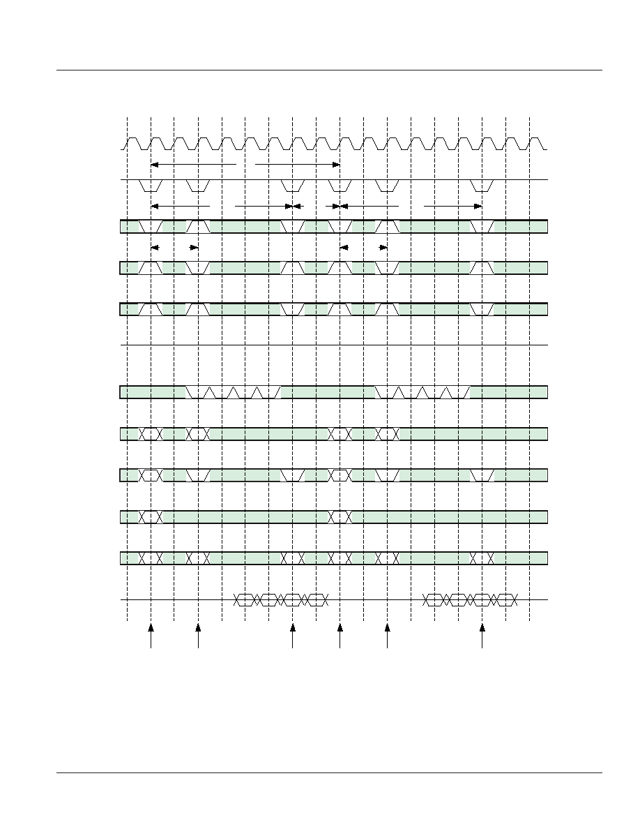
Burst Write (Single Bank) [BL=4]
0
1
4
7
9
10 11 12 13 14 15 16
X
X
X
0
Y
0
D0
D0
D0
D0
0
X
Y
X
X
0
0
D0
D0
D0
D0
0
tRC
tRCD
tRAS
tWR
tRP
tRCD
tWR
3
2
6
5
8
CLK
/CS
/RAS
/CAS
/WE
CKE
DQM
A0-9,11
A10
A12
BA0,1
DQ
ACT#0 WRITE#0
PRE#0
ACT#0 WRITE#0
PRE#0
Italic paramater
shows minimum case
34
Integrated Silicon Solution, Inc. -- 1-800-379-4774
Rev. D
11/01/05
ISSI
Æ
IS42S83200A
(4-bank x 8,388,608 - word x 8-bit)
IS42S16160A
(4-bank x 4,194,304 - word x 16-bit)
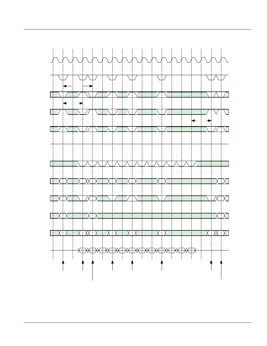
Burst Write (Multi Bank) [BL=4]
0
1
4
7
9
10 11 12 13 14 15 16
X
X
X
0
Y
0
D0
D0
D0
D0
0
X
Y
X
X
0
0
D0
D0
D0
D0
0
tRC
tRCD
tRAS
tWR
tRP
tRCD
tWR
X
X
X
1
tRRD
tRCD
Y
1
D1
D1
D1
D1
X
X
X
1
tRC
3
2
6
5
8
CLK
/CS
/RAS
/CAS
/WE
CKE
DQM
A0-9,11
A10
A12
BA0,1
DQ
ACT#0 WRITE#0
PRE#0
ACT#0
WRITE#0
PRE#0
ACT#1
WRITEA#1
ACT#1
(Auto-Precharge)
Italic paramater
shows minimum case
Integrated Silicon Solution, Inc. -- 1-800-379-4774
35
Rev. D
11/01/05
ISSI
Æ
IS42S83200A
(4-bank x 8,388,608 - word x 8-bit)
IS42S16160A
(4-bank x 4,194,304 - word x 16-bit)
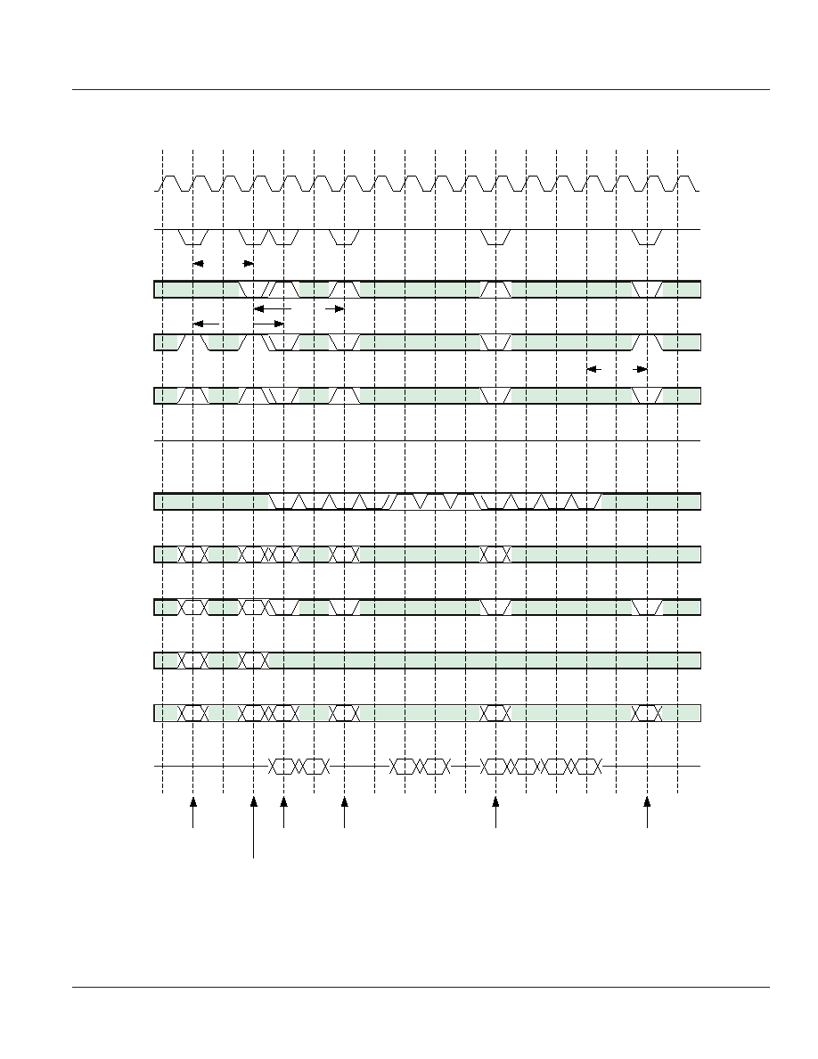
Burst Read (Single Bank) [CL=2, BL=4]
0
1
4
7
9
10 11 12 13 14 15 16
X
X
X
0
Y
0
Q0 Q0 Q0 Q0
0
X
Y
X
X
0
0
Q0 Q0 Q0 Q0
0
tRC
tRCD
tRAS
tRP
tRCD
tRAS
3
2
6
5
8
CLK
/CS
/RAS
/CAS
/WE
CKE
DQM
A0-9,11
A10
A12
BA0,1
DQ
ACT#0 READ#0
PRE#0
ACT#0 READ#0
PRE#0
Italic paramater
shows minimum case

36
Integrated Silicon Solution, Inc. -- 1-800-379-4774
Rev. D
11/01/05
ISSI
Æ
IS42S83200A
(4-bank x 8,388,608 - word x 8-bit)
IS42S16160A
(4-bank x 4,194,304 - word x 16-bit)
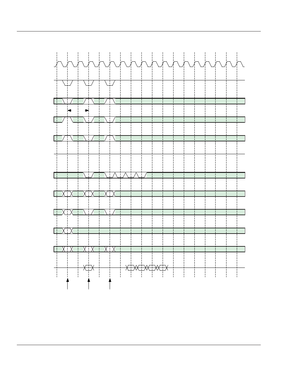
Burst Read (Multi Bank) [CL=2, BL=4]
0
1
4
7
9
10 11 12 13 14 15 16
X
X
X
0
Y
0
Q0 Q0 Q0 Q0
1
X
Y
X
X
0
0
Q0 Q0 Q0 Q0
0
tRC
tRCD
tRCD
X
X
X
1
tRRD
Y
Q1 Q1 Q1 Q1
tRCD
X
X
X
1
tRC
tRAS
3
2
6
5
8
CLK
/CS
/RAS
/CAS
/WE
CKE
DQM
A0-9,11
A10
A12
BA0,1
DQ
ACT#0 READA#0
ACT#0 READ#0
PRE#0
ACT#1
READA#1
ACT#1
Italic paramater
shows minimum case
Integrated Silicon Solution, Inc. -- 1-800-379-4774
37
Rev. D
11/01/05
ISSI
Æ
IS42S83200A
(4-bank x 8,388,608 - word x 8-bit)
IS42S16160A
(4-bank x 4,194,304 - word x 16-bit)
Write Interrupted by Write [BL=4]
0
1
4
7
9
10 11 12 13 14 15 16
X
X
X
0
Y
0
D0
D0
D0
D0
1
Y
0
D0
D0
D0
D0
0
tRCD
X
X
X
1
tRRD
Y
D0
D1
D1
D1
X
X
X
1
Y
0
tWR
3
2
6
5
8
CLK
/CS
/RAS
/CAS
/WE
CKE
DQM
A0-9,11
A10
A12
BA0,1
DQ
ACT#0 WRITE#0
WRITE#0 WRITEA#1
WRITE#0
PRE#0
interrupt
interrupt
interrupt
ACT#1
same bank other bank
other bank
ACT#1
Italic paramater
shows minimum case

38
Integrated Silicon Solution, Inc. -- 1-800-379-4774
Rev. D
11/01/05
ISSI
Æ
IS42S83200A
(4-bank x 8,388,608 - word x 8-bit)
IS42S16160A
(4-bank x 4,194,304 - word x 16-bit)
Read Interrupted by Read [CL=2, BL=4]
0
1
4
7
9
10 11 12 13 14 15 16
X
X
X
0
Y
0
Q0 Q0
1
Y
0
Q1 Q1 Q0 Q0
tRCD
X
X
X
1
tRRD
Y
Q0 Q1 Q1 Q1
X
X
X
1
Y
1
tRCD
Q0 Q0
3
2
6
5
8
CLK
/CS
/RAS
/CAS
/WE
CKE
DQM
A0-9,11
A10
A12
BA0,1
DQ
ACT#0 READ#0
READ#1
READA#1
READ#0
interrupt
interrupt
interrupt
ACT#1 other bank same bank other bank
ACT#1
Italic paramater
shows minimum case
Integrated Silicon Solution, Inc. -- 1-800-379-4774
39
Rev. D
11/01/05
ISSI
Æ
IS42S83200A
(4-bank x 8,388,608 - word x 8-bit)
IS42S16160A
(4-bank x 4,194,304 - word x 16-bit)
Write Interrupted by Read, Read Interrupted by Write [CL=2, BL=4]
0
1
4
7
9
10 11 12 13 14 15 16
X
X
X
0
Y
0
D0
D0
Y
1
D1
D1
D1
D1
1
tRCD
X
X
X
1
tRRD
Q1 Q1
Y
1
tWR
tRCD
3
2
6
5
8
CLK
/CS
/RAS
/CAS
/WE
CKE
DQM
A0-9,11
A10
A12
BA0,1
DQ
ACT#0
WRITE#0 READ#1
WRITE#1
PRE#1
ACT#1
Italic paramater
shows minimum case

40
Integrated Silicon Solution, Inc. -- 1-800-379-4774
Rev. D
11/01/05
ISSI
Æ
IS42S83200A
(4-bank x 8,388,608 - word x 8-bit)
IS42S16160A
(4-bank x 4,194,304 - word x 16-bit)
Write / Read Terminated by Precharge [CL=2, BL=4]
0
1
4
7
9
10 11 12 13 14 15 16
X
X
X
0
Y
0
D0
D0
Y
0
Q0 Q0
0
tRCD
0
tWR
X
X
X
0
tRP
0
tRAS
tRCD
tRP
X
X
X
tRC
3
2
6
5
8
CLK
/CS
/RAS
/CAS
/WE
CKE
DQM
A0-9,11
A10
A12
BA0,1
DQ
ACT#0
WRITE#0
PRE#0 ACT#0
READ#0
PRE#0
ACT#0
Terminate
Terminate
Italic paramater
shows minimum case

Integrated Silicon Solution, Inc. -- 1-800-379-4774
41
Rev. D
11/01/05
ISSI
Æ
IS42S83200A
(4-bank x 8,388,608 - word x 8-bit)
IS42S16160A
(4-bank x 4,194,304 - word x 16-bit)
Write / Read Terminated by Burst Terminate [CL=2, BL=4]
0
1
4
7
9
10 11 12 13 14 15 16
X
X
X
0
Y
0
D0
D0
Y
0
Q0 Q0
0
tRCD
Y
0
D0
D0
D0
D0
tWR
3
2
6
5
8
CLK
/CS
/RAS
/CAS
/WE
CKE
DQM
A0-9,11
A10
A12
BA0,1
DQ
ACT#0 WRITE#0 TBST READ#0 TBST
WRITE#0
PRE#0
Italic paramater
shows minimum case
42
Integrated Silicon Solution, Inc. -- 1-800-379-4774
Rev. D
11/01/05
ISSI
Æ
IS42S83200A
(4-bank x 8,388,608 - word x 8-bit)
IS42S16160A
(4-bank x 4,194,304 - word x 16-bit)
Single Write Burst Read [CL=2, BL=4]
0
1
4
7
9
10 11 12 13 14 15 16
X
X
X
0
Y
0
D0
Q0 Q0
tRCD
Q0 Q0
Y
0
3
2
6
5
8
CLK
/CS
/RAS
/CAS
/WE
CKE
DQM
A0-9,11
A10
A12
BA0,1
DQ
ACT#0 WRITE#0 READ#0
Italic paramater
shows minimum case

Integrated Silicon Solution, Inc. -- 1-800-379-4774
43
Rev. D
11/01/05
ISSI
Æ
IS42S83200A
(4-bank x 8,388,608 - word x 8-bit)
IS42S16160A
(4-bank x 4,194,304 - word x 16-bit)
Power-Up Sequence and Intialize
CLK
0
0
0
0
MA
X
X
X
200
µ
s
tRP
tRFC
tRFC
tRSC
/CS
/RAS
/CAS
/WE
CKE
DQM
A0-9,11
A10
A12
BA0,1
DQ
NOP
Power On
PRE ALL
REFA
REFA
REFA
MRS
ACT#0
Minimum 8 REFA cycles
Italic paramater
shows minimum case

44
Integrated Silicon Solution, Inc. -- 1-800-379-4774
Rev. D
11/01/05
ISSI
Æ
IS42S83200A
(4-bank x 8,388,608 - word x 8-bit)
IS42S16160A
(4-bank x 4,194,304 - word x 16-bit)
Auto Refresh
0
1
4
7
9
10 11 12 13 14 15 16
Y
0
D0
D0
D0
D0
X
X
X
0
tRP
tRFC
tRCD
3
2
6
5
8
CLK
/CS
/RAS
/CAS
/WE
CKE
DQM
A0-9,11
A10
A12
BA0,1
DQ
PRE ALL
REFA
ACT#0 WRITE#0
All banks must be idle before REFA is issued.
Italic paramater
shows minimum case

Integrated Silicon Solution, Inc. -- 1-800-379-4774
45
Rev. D
11/01/05
ISSI
Æ
IS42S83200A
(4-bank x 8,388,608 - word x 8-bit)
IS42S16160A
(4-bank x 4,194,304 - word x 16-bit)
Self Refresh
0
1
4
7
9
10 11 12 13 14 15 16
X
X
X
0
tRP
tRFC
3
2
6
5
8
CLK
/CS
/RAS
/CAS
/WE
CKE
DQM
A0-9,11
A10
A12
BA0,1
DQ
PRE ALL Self Refresh Entry
Self Refresh Exit
ACT#0
All banks must be idle before REFS is issued.
Italic paramater
shows minimum case

46
Integrated Silicon Solution, Inc. -- 1-800-379-4774
Rev. D
11/01/05
ISSI
Æ
IS42S83200A
(4-bank x 8,388,608 - word x 8-bit)
IS42S16160A
(4-bank x 4,194,304 - word x 16-bit)
CLK Suspension [CL=2, BL=4]
0
1
4
7
9
10 11 12 13 14 15 16
X
X
X
0
Y
0
D0
Q0 Q0
tRCD
Q0
Y
0
D0
D0
D0
Q0
3
2
6
5
8
CLK
/CS
/RAS
/CAS
/WE
CKE
DQM
A0-9,11
A10
A12
BA0,1
DQ
ACT#0 WRITE#0 internal CLK
READ#0
internal CLK
suspended
suspended
Italic paramater
shows minimum case

Integrated Silicon Solution, Inc. -- 1-800-379-4774
47
Rev. D
11/01/05
ISSI
Æ
IS42S83200A
(4-bank x 8,388,608 - word x 8-bit)
IS42S16160A
(4-bank x 4,194,304 - word x 16-bit)
Power Down
0
1
4
7
9
10 11 12 13 14 15 16
X
0
X
X
Standby Power Down
Active Power Down
3
2
6
5
8
CLK
/CS
/RAS
/CAS
/WE
CKE
DQM
A0-9,11
A10
A12
BA0,1
DQ
PRE ALL
ACT#0
Italic paramater
shows minimum case

48
Integrated Silicon Solution, Inc. -- 1-800-379-4774
Rev. D
11/01/05
ISSI
Æ
IS42S83200A
(4-bank x 8,388,608 - word x 8-bit)
IS42S16160A
(4-bank x 4,194,304 - word x 16-bit)
ORDERING INFORMATION
Commercial Range: 0∞C to +70∞C
Frequency
Speed (ns)
Order Part No.
Package
166 MHz
6
IS42S16160A-6T
54-pin TSOP-II
143 MHz
7
IS42S16160A-7T
54-pin TSOP-II
133 MHz
7.5
IS42S83200A-75T
54-pin TSOP-II
Commercial Range: 0∞C to +70∞C, Lead-free
Frequency
Speed (ns)
Order Part No.
Package
166 MHz
6
IS42S16160A-6TL
54-pin TSOP-II
143 MHz
7
IS42S16160A-7TL
54-pin TSOP-II
133 MHz
7.5
IS42S83200A-75TL
54-pin TSOP-II

PACKAGING INFORMATION
ISSI
Æ
Integrated Silicon Solution, Inc. -- 1-800-379-4774
1
Rev. C
01/28/02
Plastic TSOP 54≠Pin, 86-Pin
Package Code: T (Type II)
Plastic TSOP (T - Type II)
Millimeters
Inches
Symbol
Min
Max
Min
Max
Ref. Std.
No. Leads (N)
54
A
--
1.20
--
0.047
A1
0.05
0.15
0.002
0.006
A2
--
--
--
--
b
0.30
0.45
0.012
0.018
C
0.12
0.21
0.005
0.0083
D
22.02 22.42
0.867
0.8827
E1
10.03 10.29
0.395
0.405
E
11.56 11.96
0.455
0.471
e
0.80 BSC
0.031 BSC
L
0.40
0.60
0.016
0.024
L1
--
--
--
--
ZD 0.71 REF
0∞
8∞
0∞
8∞
D
SEATING PLANE
b
e
C
1
N/2
N/2+1
N
E1
A1
A
E
L
ZD
Notes:
1. Controlling dimension: millimieters,
unless otherwise specified.
2. BSC = Basic lead spacing between
centers.
3. Dimensions D and E1 do not include
mold flash protrusions and
should be
measured from the bottom of the
package
.
4. Formed leads shall be planar with
respect to one another within 0.004
inches at the seating plane.
Plastic TSOP (T - Type II)
Millimeters
Inches
Symbol
Min
Max
Min
Max
Ref. Std.
No. Leads (N)
86
A
--
1.20
--
0.047
A1
0.05
0.15
0.002
0.006
A2
0.95
1.05
0.037
0.041
b
0.17
0.27
0.007
0.011
C
0.12
0.21
0.005
0.008
D
22.02 22.42
0.867
0.8827
E1
10.16 BSC
0.400 BSC
E
11.56 11.96
0.455
0.471
e
0.50 BSC
0.020 BSC
L
0.40
0.60
0.016
0.024
L1
0.80 REF
0.031 REF
ZD 0.61 REF 0.024 BSC
0∞
8∞
0∞
8∞