
Integrated Silicon Solution, Inc. -- 1-800-379-4774
1
Rev. B
08/25/05
IS61LF6436A
IS61LF6432A
ISSI
Æ
Copyright © 2005 Integrated Silicon Solution, Inc. All rights reserved. ISSI reserves the right to make changes to this specification and its products at any time
without notice. ISSI assumes no liability arising out of the application or use of any information, products or services described herein. Customers are advised to
obtain the latest version of this device specification before relying on any published information and before placing orders for products.
FEATURES
∑ Internal self-timed write cycle
∑ Individual Byte Write Control and Global Write
∑ Clock controlled, registered address, data and
control
∑ Interleaved or linear burst sequence control
using MODE input
∑ Three chip enables for simple depth expansion
and address pipelining
∑ Common data inputs and data outputs
∑ Power-down control by ZZ input
∑ JEDEC 100-Pin TQFP package
∑ Power Supply:
+3.3V V
DD
+3.3V or 2.5V V
DDQ
∑ Control pins mode upon power-up:
≠ MODE in interleave burst mode
≠ ZZ in normal operation mode
∑ Industrial Temperature Available:
(-40
o
C to +85
o
C)
∑ Lead-free available
DESCRIPTION
The
ISSI
IS61LF6432A and IS61LF6436A are high-speed,
low-power synchronous static RAM designed to provide a
burstable, high-performance, memory. IS61LF6432A is
organized as 65,536 words by 32 bits. IS61LF6436A is
organized as 65,536 words by 36 bits. They are fabricated
with
ISSI
's advanced CMOS technology. The device inte-
grates a 2-bit burst counter, high-speed SRAM core, and
high-drive capability outputs into a single monolithic circuit.
All synchronous inputs pass through registers controlled
by a positive-edge-triggered single clock input.
Write cycles are internally self-timed and are initiated by the
rising edge of the clock input. Write cycles can be from one
to four bytes wide as controlled by the write control inputs.
Separate byte enables allow individual bytes to be written.
BWa
controls DQa,
BWb
controls DQb,
BWc
controls DQc,
BWd
controls DQd, conditioned by
BWE
being LOW. A
LOW on
GW
input would cause all bytes to be written.
Bursts can be initiated with either
ADSP
(Address Status
Processor) or
ADSC
(Address Status Cache Controller)
input pins. Subsequent burst addresses can be generated
internally by the IS61LF6432A/36A and controlled by the
ADV
(burst address advance) input pin.
The mode pin is used to select the burst sequence order.
Linear burst is achieved when this pin is tied LOW. Inter-
leave burst is achieved when this pin is tied HIGH or left
floating.
64K x 32, 64Kx36
SYNCHRONOUS FLOW-THROUGH
STATIC RAM
OCTOBER 2005
FAST ACCESS TIME
Symbol
Parameter
8.5
Unit
t
KQ
Clock Access Time
8.5
ns
t
KC
Cycle Time
11
ns
Frequency
90
MHz
IS61LF6436A
IS61LF6432A
ISSI
Æ
2
Integrated Silicon Solution, Inc. -- 1-800-379-4774
Rev. B
08/25/05
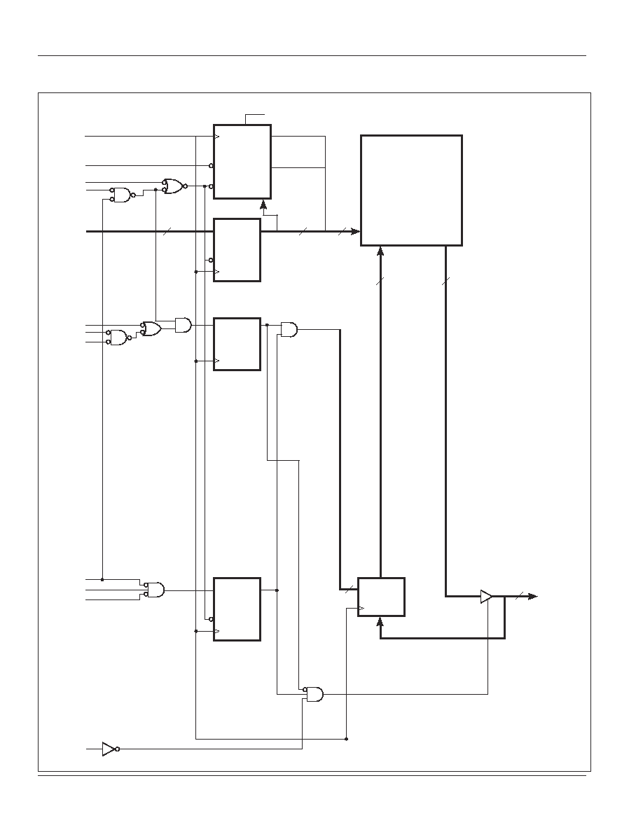
BLOCK DIAGRAM
17/18
BINARY
COUNTER
GW
CLR
CE
CLK
Q0
Q1
MODE
A0'
A1'
CLK
ADV
ADSC
ADSP
14
16
ADDRESS
REGISTER
CE
D
CLK
Q
DQ(a-d)
BYTE WRITE
REGISTERS
D
CLK
Q
ENABLE
REGISTER
CE
D
CLK
Q
BWE
BW(a-d)
x32/x36: a-d
CE
CE2
CE2
64Kx32;
64Kx36
MEMORY ARRAY
32, 36
INPUT
REGISTERS
CLK
OE
4
OE
DQa - DQd
32, 36
32, 36
A
A0, A1
IS61LF6436A
IS61LF6432A
ISSI
Æ
Integrated Silicon Solution, Inc. -- 1-800-379-4774
3
Rev. B
08/25/05
PIN CONFIGURATION
PIN DESCRIPTIONS
A0, A1
Synchronous Address Inputs. These
pins must tied to the two LSBs of the
address bus.
A
Synchronous Address Inputs
CLK
Synchronous Clock
ADSP
Synchronous Processor Address
Status
ADSC
Synchronous Controller Address
Status
ADV
Synchronous Burst Address Advance
BWa
-
BWd
Individual Byte Write Enable
BWE
Synchronous Byte Write Enable
GW
Synchronous Global Write Enable
CE
,
CE2
, CE2 Synchronous Chip Enable
OE
Output Enable
DQa-DQd
Synchronous Data Input/Output
MODE
Burst Sequence Mode Selection
V
DD
+3.3V Power Supply
Vss
Ground
V
DDQ
Isolated Output Buffer Supply: +3.3V
or 2.5V
ZZ
Snooze Enable
NC
DQb
DQb
VDDQ
Vss
DQb
DQb
DQb
DQb
Vss
VDDQ
DQb
DQb
Vss
NC
VDD
ZZ
DQa
DQa
VDDQ
Vss
DQa
DQa
DQa
DQa
Vss
VDDQ
DQa
DQa
NC
A
A
CE
CE2
BWd
BWc
BWb
BWa
CE2
VDD
Vss
CLK
GW
BWE
OE
ADS
C
ADSP
ADV
A
A
NC
DQc
DQc
VDDQ
Vss
DQc
DQc
DQc
DQc
Vss
VDDQ
DQc
DQc
NC
VDD
NC
Vss
DQd
DQd
VDDQ
Vss
DQd
DQd
DQd
DQd
Vss
VDDQ
DQd
DQd
NC
1
2
3
4
5
6
7
8
9
10
11
12
13
14
15
16
17
18
19
20
21
22
23
24
25
26
27
28
29
30
80
79
78
77
76
75
74
73
72
71
70
69
68
67
66
65
64
63
62
61
60
59
58
57
56
55
54
53
52
51
100 99 98 97 96 95 94 93 92 91 90 89 88 87 86 85 84 83 82 81
31 32 33 34 35 36 37 38 39 40 41 42 43 44 45
MODE
A
A
A
A
A1
A0
NC
NC
Vss
VDD
NC
NC
A
A
A
A
A
A
NC
46 47 48 49 50
64K x 32
100-Pin TQFP
IS61LF6436A
IS61LF6432A
ISSI
Æ
4
Integrated Silicon Solution, Inc. -- 1-800-379-4774
Rev. B
08/25/05
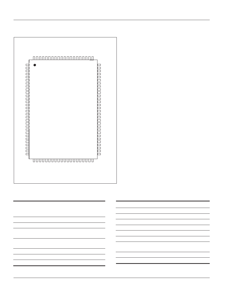
PIN CONFIGURATION
PIN DESCRIPTIONS
A0, A1
Synchronous Address Inputs. These
pins must tied to the two LSBs of the
address bus.
A
Synchronous Address Inputs
CLK
Synchronous Clock
ADSP
Synchronous Processor Address
Status
ADSC
Synchronous Controller Address
Status
ADV
Synchronous Burst Address Advance
BWa
-
BWd
Individual Byte Write Enable
BWE
Synchronous Byte Write Enable
GW
Synchronous Global Write Enable
CE
,
CE2
, CE2 Synchronous Chip Enable
OE
Output Enable
DQa-DQd
Synchronous Data Input/Output
MODE
Burst Sequence Mode Selection
V
DD
+3.3V Power Supply
Vss
Ground
V
DDQ
Isolated Output Buffer Supply: +3.3V or
2.5V
ZZ
Snooze Enable
DQPa-DQPd
Parity Data I/O
DQPb
DQb
DQb
VDDQ
Vss
DQb
DQb
DQb
DQb
Vss
VDDQ
DQb
DQb
Vss
NC
VDD
ZZ
DQa
DQa
VDDQ
Vss
DQa
DQa
DQa
DQa
Vss
VDDQ
DQa
DQa
DQPa
A
A
CE
CE2
BWd
BWc
BWb
BWa
CE2
VDD
Vss
CLK
GW
BWE
OE
ADS
C
ADSP
ADV
A
A
DQPc
DQc
DQc
VDDQ
Vss
DQc
DQc
DQc
DQc
Vss
VDDQ
DQc
DQc
NC
VDD
NC
Vss
DQd
DQd
VDDQ
Vss
DQd
DQd
DQd
DQd
Vss
VDDQ
DQd
DQd
DQPd
1
2
3
4
5
6
7
8
9
10
11
12
13
14
15
16
17
18
19
20
21
22
23
24
25
26
27
28
29
30
80
79
78
77
76
75
74
73
72
71
70
69
68
67
66
65
64
63
62
61
60
59
58
57
56
55
54
53
52
51
100 99 98 97 96 95 94 93 92 91 90 89 88 87 86 85 84 83 82 81
31 32 33 34 35 36 37 38 39 40 41 42 43 44 45
MODE
A
A
A
A
A1
A0
NC
NC
Vss
VDD
NC
NC
A
A
A
A
A
A
NC
46 47 48 49 50
64K x 36
100-Pin TQFP

IS61LF6436A
IS61LF6432A
ISSI
Æ
Integrated Silicon Solution, Inc. -- 1-800-379-4774
5
Rev. B
08/25/05
TRUTH TABLE
Address
Operation
Used
CE
CE
CE
CE
CE
CE2
CE2
CE2
CE2
CE2
CE2
ADSP
ADSP
ADSP
ADSP
ADSP ADSC
ADSC
ADSC
ADSC
ADSC
ADV
ADV
ADV
ADV
ADV WRITE
WRITE
WRITE
WRITE
WRITE
OE
OE
OE
OE
OE
DQ
Deselected, Power-down
None
H
X
X
X
L
X
X
X
High-Z
Deselected, Power-down
None
L
X
H
L
X
X
X
X
High-Z
Deselected, Power-down
None
L
L
X
L
X
X
X
X
High-Z
Deselected, Power-down
None
X
X
H
H
L
X
X
X
High-Z
Deselected, Power-down
None
X
L
X
H
L
X
X
X
High-Z
Read Cycle, Begin Burst
External
L
H
L
L
X
X
X
X
Q
Read Cycle, Begin Burst
External
L
H
L
H
L
X
Read
X
Q
Write Cycle, Begin Burst
External
L
H
L
H
L
X
Write
X
D
Read Cycle, Continue Burst
Next
X
X
X
H
H
L
Read
L
Q
Read Cycle, Continue Burst
Next
X
X
X
H
H
L
Read
H
High-Z
Read Cycle, Continue Burst
Next
H
X
X
X
H
L
Read
L
Q
Read Cycle, Continue Burst
Next
H
X
X
X
H
L
Read
H
High-Z
Write Cycle, Continue Burst
Next
X
X
X
H
H
L
Write
X
D
Write Cycle, Continue Burst
Next
H
X
X
X
H
L
Write
X
D
Read Cycle, Suspend Burst
Current
X
X
X
H
H
H
Read
L
Q
Read Cycle, Suspend Burst
Current
X
X
X
H
H
H
Read
H
High-Z
Read Cycle, Suspend Burst
Current
H
X
X
X
H
H
Read
L
Q
Read Cycle, Suspend Burst
Current
H
X
X
X
H
H
Read
H
High-Z
Write Cycle, Suspend Burst
Current
X
X
X
H
H
H
Write
X
D
Write Cycle, Suspend Burst
Current
H
X
X
X
H
H
Write
X
D
PARTIAL TRUTH TABLE
Function
GW
GW
GW
GW
GW
BWE
BWE
BWE
BWE
BWE
BWa
BWa
BWa
BWa
BWa
BWb
BWb
BWb
BWb
BWb
BWc
BWc
BWc
BWc
BWc
BWd
BWd
BWd
BWd
BWd
Read
H
H
X
X
X
X
Read
H
L
H
H
H
H
Write Byte 1
H
L
L
H
H
H
Write All Bytes
H
L
L
L
L
L
Write All Bytes
L
X
X
X
X
X
IS61LF6436A
IS61LF6432A
ISSI
Æ
6
Integrated Silicon Solution, Inc. -- 1-800-379-4774
Rev. B
08/25/05
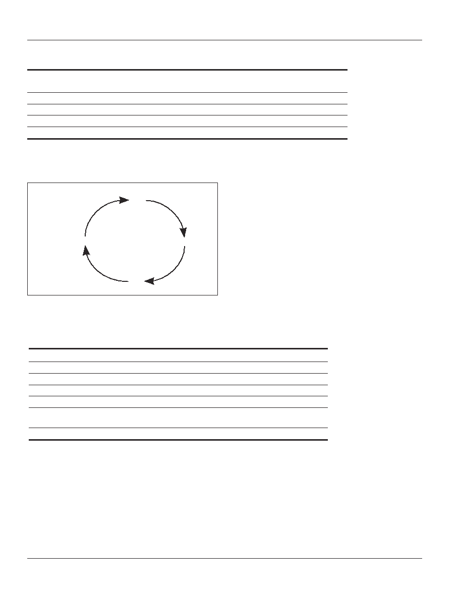
INTERLEAVED BURST ADDRESS TABLE (MODE = V
DD
or No Connect)
External Address
1st Burst Address
2nd Burst Address
3rd Burst Address
A1 A0
A1 A0
A1 A0
A1 A0
00
01
10
11
01
00
11
10
10
11
00
01
11
10
01
00
ABSOLUTE MAXIMUM RATINGS
(1)
Symbol
Parameter
Value
Unit
T
STG
Storage Temperature
≠55 to +150
∞C
P
D
Power Dissipation
1.6
W
I
OUT
Output Current (per I/O)
100
mA
V
IN
, V
OUT
Voltage Relative to Vss for I/O Pins
≠0.5 to V
DDQ
+ 0.3
V
V
IN
Voltage Relative to Vss for
≠0.5 to V
DD
+ 0.5
V
for Address and Control Inputs
V
DD
Voltage on V
DD
Supply Relative to Vss
≠0.5 to 4.6
V
Notes:
1. Stress greater than those listed under ABSOLUTE MAXIMUM RATINGS may cause permanent
damage to the device. This is a stress rating only and functional operation of the device at these
or any other conditions above those indicated in the operational sections of this specification
is not implied. Exposure to absolute maximum rating conditions for extended periods may
affect reliability.
2. This device contains circuitry to protect the inputs against damage due to high static voltages
or electric fields; however, precautions may be taken to avoid application of any voltage higher
than maximum rated voltages to this high-impedance circuit.
3. This device contains circuitry that will ensure the output devices are in High-Z at power up.
0,0
1,0
0,1
A1', A0' = 1,1

IS61LF6436A
IS61LF6432A
ISSI
Æ
Integrated Silicon Solution, Inc. -- 1-800-379-4774
7
Rev. B
08/25/05
DC ELECTRICAL CHARACTERISTICS
(1)
(Over Operating Range)
2.5V (I/O)
3.3V (I/O)
Symbol
Parameter
Test Conditions
Min.
Max.
Min.
Max.
Unit
V
OH
Output HIGH Voltage
I
OH
= ≠4.0 mA (3.3V)
2.0
--
2.4
--
V
I
OH
= 1.0 mA (2.5V)
V
OL
Output LOW Voltage
I
OL
= 8.0 mA (3.3V)
--
0.4
--
0.4
V
I
OL
= 1.0 mA (2.5V)
V
IH
Input HIGH Voltage
1.7
V
DD
+ 0.3
2.0
V
DD
+ 0.3
V
V
IL
Input LOW Voltage
≠0.3
0.7
≠0.3
0.8
V
I
LI
Input Leakage Current
Vss
V
IN
V
DD
≠5
5
≠5
5
µA
I
LO
Output Leakage Current
Vss
V
OUT
V
DDQ
,
≠5
5
≠5
5
µA
OE
= V
I
POWER SUPPLY CHARACTERISTICS
(Over Operating Range)
8.5
Symbol
Parameter
Test Conditions
Max.
Unit
I
CC
AC Operating
Device Selected,
I
ND
.
150
mA
Supply Current
OE
= V
IH
, ZZ
V
IL
,
All Inputs
0.2V or
V
DD
≠ 0.2V,
Cycle Time
t
KC
min.
I
SB
1
Standby Current
Device Deselected,
I
ND
.
75
mA
CMOS Input
V
DD
= Max.,
V
IN
V
SS
+ 0.2V or
V
DD
≠ 0.2V
f = 0
I
ZZ
Sleep Mode
ZZ>V
IH
I
ND
.
35
mA
Notes:
1. The MODE pin has an internal pullup. This pin may be a No Connect, tied to Vss, or tied to V
DD
.
2. The MODE pin should be tied to V
DD
or Vss. It exhibits ±10 µA maximum leakage current when tied to
Vss + 0.2V
or
V
DD
≠ 0.2V.
OPERATING RANGE
3.3V (I/O)
2.5V (I/O)
Range
Ambient Temperature
V
DD
V
DDQ
V
DDQ
Industrial
≠40∞C to +85∞C
3.3V, +10%, ≠5%
3.3V, +10%, ≠5%
2.5V + 5%
IS61LF6436A
IS61LF6432A
ISSI
Æ
8
Integrated Silicon Solution, Inc. -- 1-800-379-4774
Rev. B
08/25/05
CAPACITANCE
(1,2)
Symbol
Parameter
Conditions
Max.
Unit
C
IN
Input Capacitance
V
IN
= 0V
6
pF
C
OUT
Input/Output Capacitance
V
OUT
= 0V
8
pF
Notes:
1. Tested initially and after any design or process changes that may affect these parameters.
2. Test conditions: T
A
= 25∞C, f = 1 MHz, V
DD
= 3.3V.
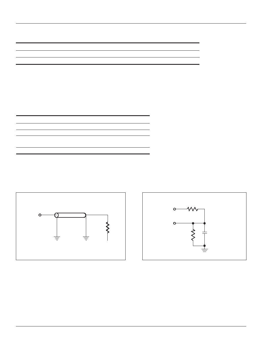
3.3V I/O AC TEST CONDITIONS
Parameter
Unit
Input Pulse Level
0V to 3.0V
Input Rise and Fall Times
1.5 ns
Input and Output Timing
1.5V
and Reference Level
Output Load
See Figures 1 and 2
Output
Z
O
= 50
1.5V
50
317
5 pF
Including
jig and
scope
351
OUTPUT
+3.3V
Figure 1
Figure 2
3.3V I/O OUTPUT LOAD EQUIVALENT
IS61LF6436A
IS61LF6432A
ISSI
Æ
Integrated Silicon Solution, Inc. -- 1-800-379-4774
9
Rev. B
08/25/05
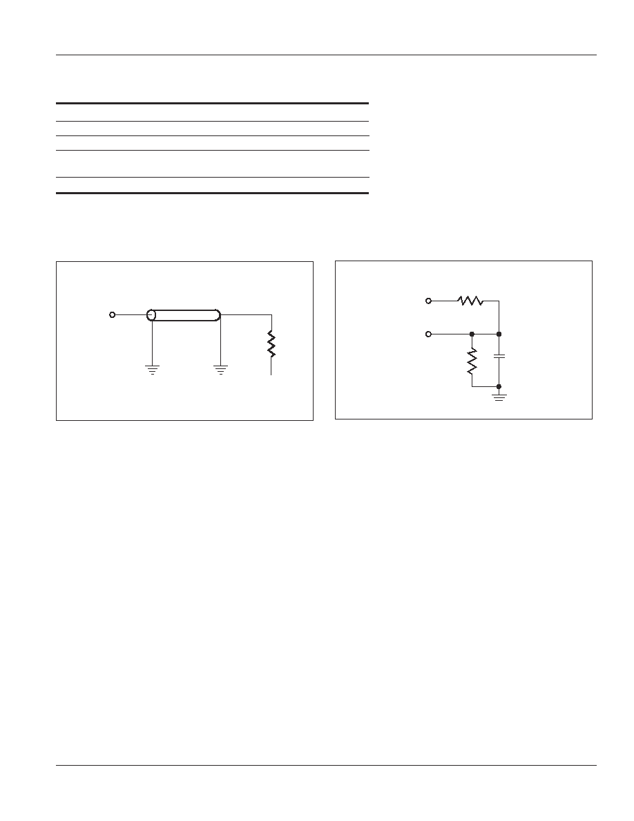
2.5V I/O AC TEST CONDITIONS
Parameter
Unit
Input Pulse Level
0V to 2.5V
Input Rise and Fall Times
1ns
Input and Output Timing
1.25V
and Reference Level
Output Load
See Figures 3 and 4
Output
Z
O
= 50
1.25V
50
1,667
5 pF
Including
jig and
scope
1538
OUTPUT
+2.5V
Figure 3
Figure 4
2.5V I/O OUTPUT LOAD EQUIVALENT

IS61LF6436A
IS61LF6432A
ISSI
Æ
10
Integrated Silicon Solution, Inc. -- 1-800-379-4774
Rev. B
08/25/05
READ/WRITE CYCLE SWITCHING CHARACTERISTICS (Over Operating Range)
8.5
Symbol
Parameter
Min.
Max.
Unit
f
MAX
(3)
Clock Frequency
--
90
MHz
t
KC
(3)
Cycle Time
11
--
ns
t
KH
Clock High Time
4.5
--
ns
t
KL
(3)
Clock Low Time
4.5
--
ns
t
KQ
(3)
Clock Access Time
--
8.5
ns
t
KQX
(1)
Clock High to Output Invalid
2
--
ns
t
KQLZ
(1,2)
Clock High to Output Low-Z
0
--
ns
t
KQHZ
(1,2)
Clock High to Output High-Z
2
3.5
ns
t
OEQ
(3)
Output Enable to Output Valid
--
4.0
ns
t
OEQX
(1)
Output Enable to Output Invalid
2
--
ns
t
OELZ
(1,2)
Output Enable to Output Low-Z
0
--
ns
t
OEHZ
(1,2)
Output Disable to Output High-Z
--
5.0
ns
t
AS
(3)
Address Setup Time
2
--
ns
t
SS
(3)
Address Status Setup Time
2
--
ns
t
WS
(3)
Write Setup Time
2
--
ns
t
CES
(3)
Chip Enable Setup Time
2
--
ns
t
AVS
(3)
Address Advance Setup Time
2
--
ns
t
AH
(3)
Address Hold Time
1
--
ns
t
SH
(3)
Address Status Hold Time
0.5
--
ns
t
WH
(3)
Write Hold Time
0.5
--
ns
t
CEH
(3)
Chip Enable Hold Time
0.5
--
ns
t
AVH
(3)
Address Advance Hold Time
0.5
--
ns
Notes:
1. Guaranteed but not 100% tested. This parameter is periodically sampled.
2. Tested with load in Figure 2.
3. Tested with load in Figure 1.
IS61LF6436A
IS61LF6432A
ISSI
Æ
Integrated Silicon Solution, Inc. -- 1-800-379-4774
11
Rev. B
08/25/05
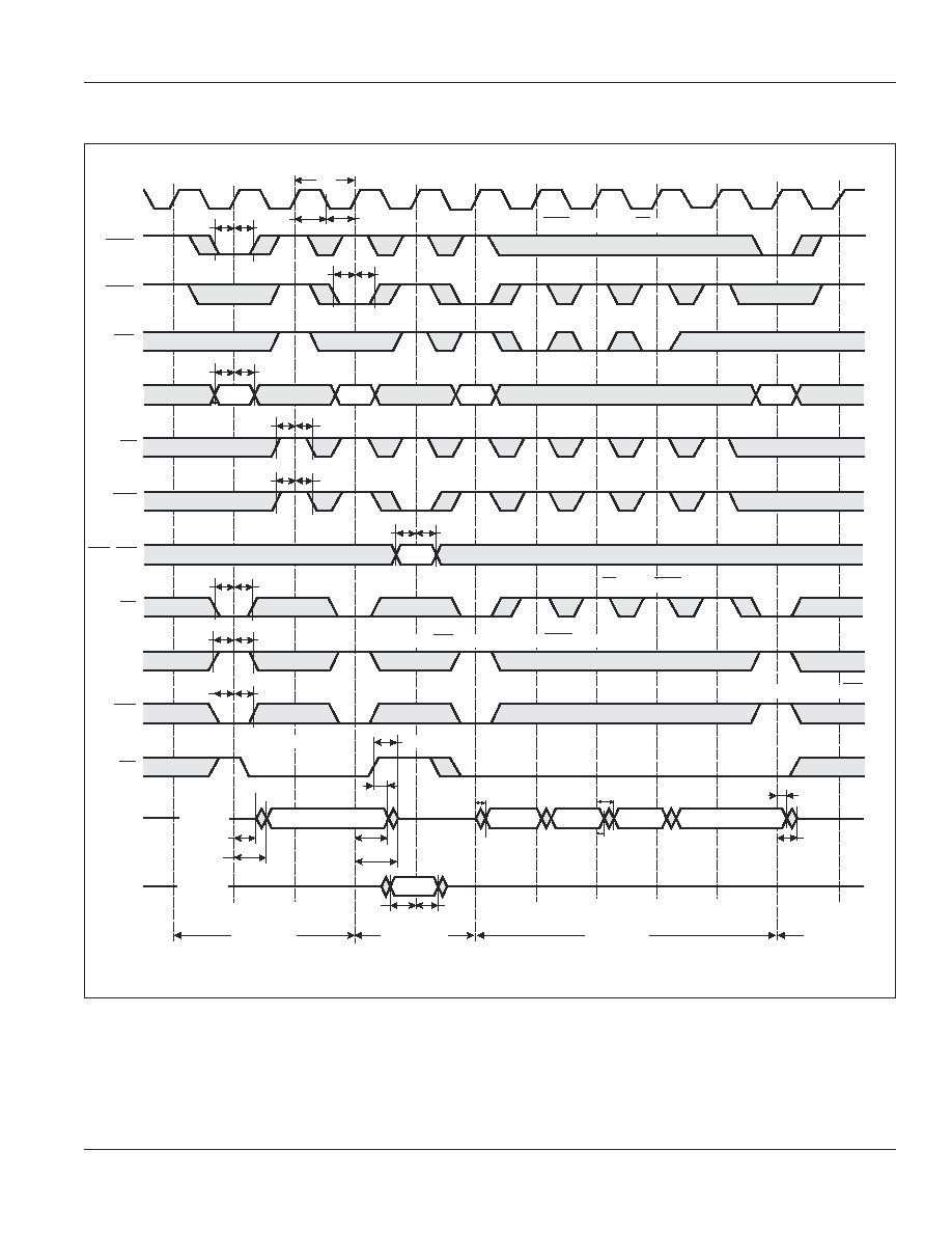
READ/WRITE CYCLE TIMING
Single Read
Flow-through
Single Write
High-Z
High-Z
DATA
OUT
DATA
IN
OE
CE2
CE2
CE
BWd-BWa
BWE
GW
Address
ADV
ADSC
ADSP
CLK
RD1
WR1
WR1
1a
1a
2a
2b
2c
2d
Unselected
Burst Read
t
KQX
t
KC
t
KL
t
KH
t
SS
t
SH
ADSP is blocked by CE inactive
t
SS
t
SH
t
AS
t
AH
t
WS
t
WH
t
WS
t
WH
t
WS
t
WH
RD2
RD3
t
CES
t
CEH
t
CES
t
CEH
t
CES
t
CEH
CE2 and CE2 only sampled with ADSP or ADSC
CE Masks ADSP
Unselected with CE2
t
OEQX
t
KQ
t
OEHZ
t
KQX
t
KQHZ
t
DS
t
DH
t
KQHZ
t
KQLZ
t
KQ
t
KQ
t
KQX

IS61LF6436A
IS61LF6432A
ISSI
Æ
12
Integrated Silicon Solution, Inc. -- 1-800-379-4774
Rev. B
08/25/05
WRITE CYCLE SWITCHING CHARACTERISTICS (Over Operating Range)
8.5
Symbol
Parameter
Min.
Max.
Unit
t
KC
(1)
Cycle Time
11
--
ns
t
KH
(1)
Clock High Time
4.5
--
ns
t
KL
(1)
Clock Low Time
4.5
--
ns
t
AS
(1)
Address Setup Time
2
--
ns
t
SS
(1)
Address Status Setup Time
2
--
ns
t
WS
(1)
Write Setup Time
2
--
ns
t
DS
(1)
Data In Setup Time
3
--
ns
t
CES
(1)
Chip Enable Setup Time
2
--
ns
t
AVS
(1)
Address Advance Setup Time
2
--
ns
t
AH
(1)
Address Hold Time
1
--
ns
t
SH
(1)
Address Status Hold Time
0.5
--
ns
t
DH
(1)
Data In Hold Time
1
--
ns
t
WH
(1)
Write Hold Time
0.5
--
ns
t
CEH
(1)
Chip Enable Hold Time
0.5
--
ns
t
AVH
(1)
Address Advance Hold Time
0.5
--
ns
Notes:
1. Tested with load in Figure 1.
IS61LF6436A
IS61LF6432A
ISSI
Æ
Integrated Silicon Solution, Inc. -- 1-800-379-4774
13
Rev. B
08/25/05
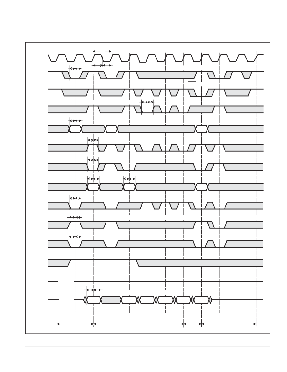
WRITE CYCLE TIMING
Single Write
DATA
OUT
DATA
IN
OE
CE2
CE2
CE
BWd
-
BWa
BWE
GW
A
ADV
ADSC
ADSP
CLK
WR1
WR2
Unselected
Burst Write
t
KC
t
KL
t
KH
t
SS
t
SH
t
AS
t
AH
t
WS
t
WH
t
WS
t
WH
WR3
t
CES
t
CEH
t
CES
t
CEH
t
CES
t
CEH
CE2 and
CE2
only sampled with
ADSP
or
ADSC
CE
Masks
ADSP
Unselected with CE2
ADSC initiate Write
ADSP is blocked by
CE
inactive
t
AVH
t
AVS
ADV
must be inactive for
ADSP
Write
WR1
WR2
t
WS
t
WH
WR3
t
WS
t
WH
High-Z
High-Z
1a
3a
t
DS
t
DH
BW4-BW1 only are applied to first cycle of WR2
Write
2c
2d
2b
2a

IS61LF6436A
IS61LF6432A
ISSI
Æ
14
Integrated Silicon Solution, Inc. -- 1-800-379-4774
Rev. B
08/25/05
SNOOZE MODE TIMING
Don't Care
Deselect or Read Only
Deselect or Read Only
t
RZZI
CLK
ZZ
Isupply
All Inputs
(except ZZ)
Outputs
(Q)
I
SB2
ZZ setup cycle
ZZ recovery cycle
Normal
operation
cycle
t
PDS
t
PUS
t
ZZI
High-Z
SNOOZE MODE ELECTRICAL CHARACTERISTICS
Symbol
Parameter
Conditions
Min.
Max.
Unit
I
SB
2
Current during SNOOZE MODE
ZZ
Vih
--
35
mA
t
PDS
ZZ active to input ignored
--
2
cycle
t
PUS
ZZ inactive to input sampled
2
--
cycle
t
ZZI
ZZ active to SNOOZE current
--
2
cycle
t
RZZI
ZZ inactive to exit SNOOZE current
0
--
ns

IS61LF6436A
IS61LF6432A
ISSI
Æ
Integrated Silicon Solution, Inc. -- 1-800-379-4774
15
Rev. B
08/25/05
ORDERING INFORMATION
3.3V I/O OR 2.5V I/O
Industrial Range: -40∞C TO +85∞C
Speed (ns)
Order Part No.
Package
8.5
IS61LF6432A-8.5TQI
TQFP
IS61LF6432A-8.5TQLI
TQFP, Lead-free
8.5
IS61LF6436A-8.5TQI
TQFP
IS61LF6436A-8.5TQLI
TQFP, Lead-free
Integrated Silicon Solution, Inc. -- 1-800-379-4774
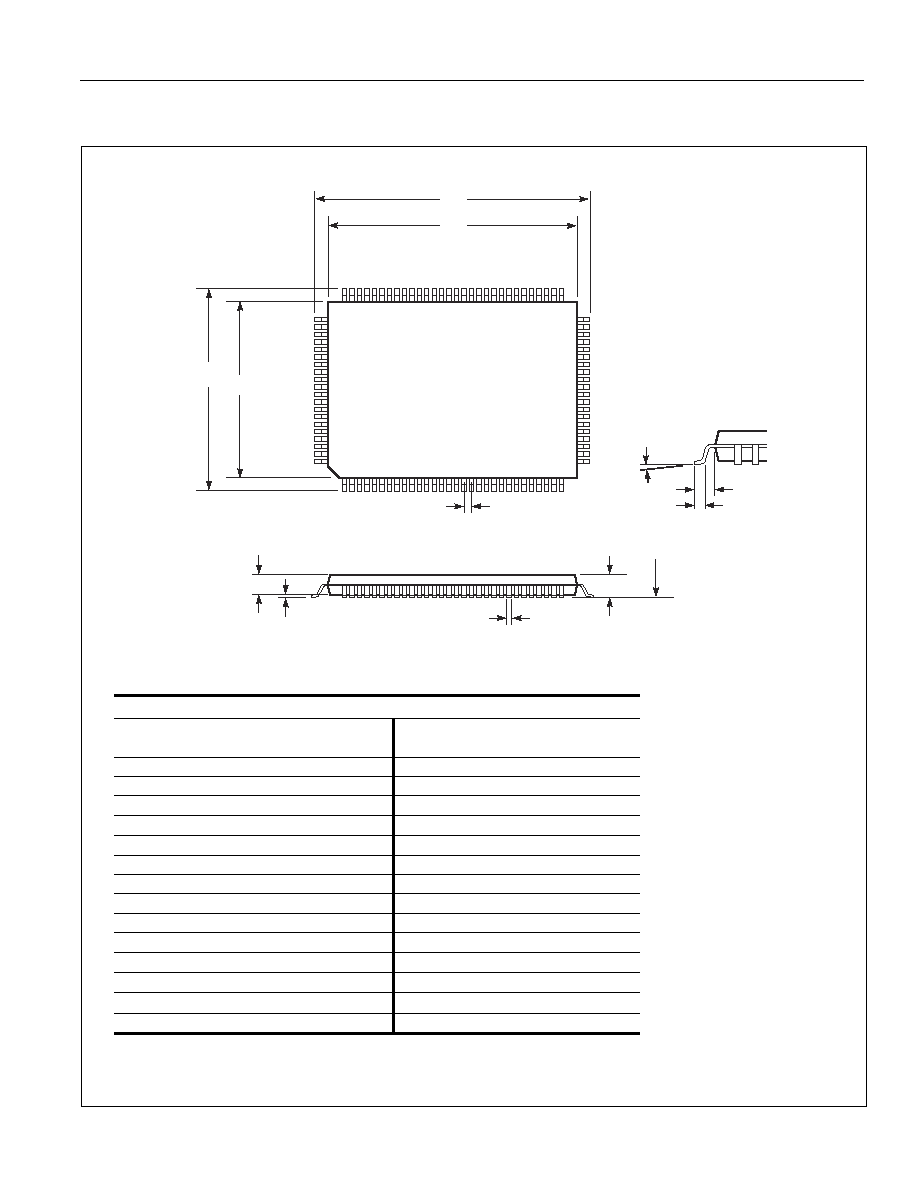
PACKAGING INFORMATION
ISSI
Æ
PK13197LQ Rev. D 05/08/03
TQFP (Thin Quad Flat Pack Package)
Package Code: TQ
Thin Quad Flat Pack (TQ)
Millimeters
Inches
Millimeters
Inches
Symbol
Min
Max
Min
Max
Min
Max
Min
Max
Ref. Std.
No. Leads (N)
100
128
A
--
1.60
--
0.063
--
1.60
--
0.063
A1
0.05
0.15
0.002
0.006
0.05
0.15
0.002
0.006
A2
1.35
1.45
0.053
0.057
1.35
1.45
0.053
0.057
b
0.22
0.38
0.009
0.015
0.17
0.27
0.007
0.011
D
21.90
22.10
0.862
0.870
21.80
22.20
0.858
0.874
D1
19.90
20.10
0.783
0.791
19.90
20.10
0.783
0.791
E
15.90
16.10
0.626
0.634
15.80
16.20
0.622
0.638
E1
13.90
14.10
0.547
0.555
13.90
14.10
0.547
0.555
e
0.65 BSC
0.026 BSC
0.50 BSC
0.020 BSC
L
0.45
0.75
0.018
0.030
0.45
0.75
0.018
0.030
L1
1.00 REF.
0.039 REF.
1.00 REF.
0.039 REF.
C
0
o
7
o
0
o
7
o
0
o
7
o
0
o
7
o
Notes:
1. All dimensioning and
tolerancing conforms to
ANSI Y14.5M-1982.
2. Dimensions D1 and E1 do
not include mold protrusions.
Allowable protrusion is 0.25
mm per side. D1 and E1 do
include mold mismatch and
are determined at datum
plane -H-.
3. Controlling dimension:
millimeters.
D
D1
E
E1
1
N
A2
A
A1
e
b
SEATING
PLANE
C
L1
L