Äîêóìåíòàöèÿ è îïèñàíèÿ www.docs.chipfind.ru

IS61SF12832
IS61SF12836
ISSI
®
Integrated Silicon Solution, Inc. -- 1-800-379-4774
1
Rev. A
04/17/01
ISSI reserves the right to make changes to its products at any time without notice in order to improve design and supply the best possible product. We assume no responsibility for any
errors which may appear in this publication. © Copyright 2001, Integrated Silicon Solution, Inc.
FEATURES
· Fast access times: 7.5 ns, 8 ns, 8.5 ns, 10 ns,
and 12 ns
· Internal self-timed write cycle
· Individual Byte Write Control and Global Write
· Clock controlled, registered address, data
inputs and control signals
· PentiumTM or linear burst sequence control
using MODE input
· Three chip enables for simple depth expansion
and address pipelining
· Common data inputs and data outputs
· JEDEC 100-Pin TQFP and
119-pin PBGA package
· Single +3.3V +10%, 5% power supply
· Power-down snooze mode
DESCRIPTION
The
ISSI
IS61SF12832 and IS61SF12836 are high-speed
synchronous static RAM designed to provide a burstable,
high-performance memory for high speed networking and
communication applications. It is organized as 131,072
words by 32 bits or 36 bits, fabricated with
ISSI
's advanced
CMOS technology. The device integrates a 2-bit burst counter,
high-speed SRAM core, and high-drive capability outputs into
a single monolithic circuit. All synchronous inputs pass
through registers controlled by a positive-edge-triggered
single clock input.
Write cycles are internally self-timed and are initiated by the
rising edge of the clock input. Write cycles can be from one to
four bytes wide as controlled by the write control inputs.
Separate byte enables allow individual bytes to be written.
BW1 controls DQa, BW2 controls DQb, BW3 controls DQc,
BW4 controls DQd, conditioned by BWE being LOW. A LOW
on
GW input would cause all bytes to be written.
Bursts can be initiated with either
ADSP (Address Status
Processor) or
ADSC (Address Status Cache Controller) input
pins. Subsequent burst addresses can be generated internally
and controlled by the
ADV (burst address advance) input pin.
The mode pin is used to select the burst sequence order,
Linear burst is achieved when this pin is tied LOW. Interleave
burst is achieved when this pin is tied HIGH or left floating.
128K x 32, 128K x 36 SYNCHRONOUS
FLOW-THROUGH STATIC RAM
APRIL 2001
FAST ACCESS TIME
Symbol
Parameter
7.5
8
8.5
10
12
Units
t
KQ
Clock Access Time
7.5
8
8.5
10
12
ns
t
KC
Cycle Time
8.5
10
11
15
15
ns
Frequency
117
100
90
66
66
MHz
IS61SF12832
IS61SF12836
ISSI
®
2
Integrated Silicon Solution, Inc. -- 1-800-379-4774
Rev. A
04/17/01
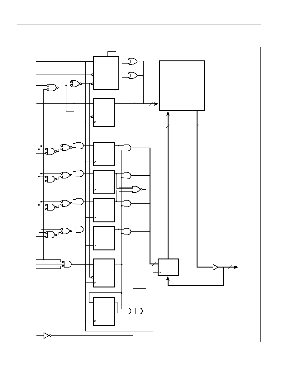
BLOCK DIAGRAM
17
BINARY
COUNTER
A16-A0
BW1
GW
CLR
CE
CLK
Q0
Q1
MODE
A0'
A0
A1
A1'
CLK
ADV
ADSC
ADSP
15
17
ADDRESS
REGISTER
CE
D
CLK
Q
DQd
BYTE WRITE
REGISTERS
D
CLK
Q
DQc
BYTE WRITE
REGISTERS
D
CLK
Q
DQb
BYTE WRITE
REGISTERS
D
CLK
Q
DQa
BYTE WRITE
REGISTERS
D
CLK
Q
ENABLE
REGISTER
CE
D
CLK
Q
ENABLE
DELAY
REGISTER
D
CLK
Q
BWE
BW4
CE
CE2
CE2
BW2
BW3
128K x 32, 128K x 36
MEMORY ARRAY
32
or
36
INPUT
REGISTERS
CLK
32
or
36
OE
4
32 or 36
OE
DQ[31:0] or
DQ[35:0]
IS61SF12832
IS61SF12836
ISSI
®
Integrated Silicon Solution, Inc. -- 1-800-379-4774
3
Rev. A
04/17/01
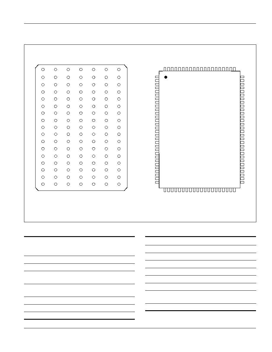
PIN CONFIGURATION
PIN DESCRIPTIONS
A0, A1
Synchronous Address Inputs. These
pins must tied to the two LSBs of the
address bus.
A2-A16
Synchronous Address Inputs
CLK
Synchronous Clock
ADSP
Synchronous Processor Address
Status
ADSC
Synchronous Controller Address
Status
ADV
Synchronous Burst Address Advance
BW1-BW4
Individual Byte Write Enable
BWE
Synchronous Byte Write Enable
GW
Synchronous Global Write Enable
CE, CE2, CE2 Synchronous Chip Enable
OE
Output Enable
DQa-DQd
Synchronous Data Input/Output
MODE
Burst Sequence Mode Selection
V
CC
+3.3V Power Supply
GND
Ground
V
CCQ
Isolated Output Buffer Supply:
+3.3V
ZZ
Snooze Enable
A
B
C
D
E
F
G
H
J
K
L
M
N
P
R
T
U
VCCQ
NC
NC
DQc1
DQc2
VCCQ
DQc5
DQc7
VCCQ
DQd1
DQd4
VCCQ
DQd6
DQd8
NC
NC
VCCQ
A6
CE2
A7
NC
DQc3
DQc4
DQc6
DQc8
VCC
DQd2
DQd3
DQd5
DQd7
NC
A5
NC
NC
A4
A3
A2
GND
GND
GND
BW3
GND
NC
GND
BW4
GND
GND
GND
MODE
A10
NC
ADSP
ADSC
VCC
NC
CE
OE
ADV
GW
VCC
CLK
NC
BWE
A1
A0
VCC
A11
NC
A8
A9
A12
GND
GND
GND
BW2
GND
NC
GND
BW1
GND
GND
GND
GND
A14
NC
A16
CE2
A15
NC
DQb6
DQb5
DQb4
DQb2
VCC
DQa7
DQa5
DQa4
DQa3
NC
A13
NC
NC
VCCQ
NC
NC
DQb8
DQb7
VCCQ
DQb3
DQb1
VCCQ
DQa8
DQa6
VCCQ
DQa2
DQa1
NC
ZZ
VCCQ
1 2 3 4 5 6 7
NC
DQb8
DQb7
VCCQ
GND
DQb6
DQb5
DQb4
DQb3
GND
VCCQ
DQb2
DQb1
GND
NC
VCC
ZZ
DQa8
DQa7
VCCQ
GND
DQa6
DQa5
DQa4
DQa3
GND
VCCQ
DQa2
DQa1
NC
A6
A7
CE
CE2
BW4
BW3
BW2
BW1
CE2
VCC
GND
CLK
GW
BWE
OE
ADSC
ADSP
ADV
A8
A9
NC
DQc1
DQc2
VCCQ
GND
DQc3
DQc4
DQc5
DQc6
GND
VCCQ
DQc7
DQc8
NC
VCC
NC
GND
DQd1
DQd2
VCCQ
GND
DQd3
DQd4
DQd5
DQd6
GND
VCCQ
DQd7
DQd8
NC
1
2
3
4
5
6
7
8
9
10
11
12
13
14
15
16
17
18
19
20
21
22
23
24
25
26
27
28
29
30
80
79
78
77
76
75
74
73
72
71
70
69
68
67
66
65
64
63
62
61
60
59
58
57
56
55
54
53
52
51
100 99 98 97 96 95 94 93 92 91 90 89 88 87 86 85 84 83 82 81
31 32 33 34 35 36 37 38 39 40 41 42 43 44 45
MODE
A5
A4
A3
A2
A1
A0
NC
NC
GND
VCC
NC
NC
A10
A11
A12
A13
A14
A15
A16
46 47 48 49 50
128K x 32
119-pin PBGA (Top View)
100-Pin TQFP
IS61SF12832
IS61SF12836
ISSI
®
4
Integrated Silicon Solution, Inc. -- 1-800-379-4774
Rev. A
04/17/01
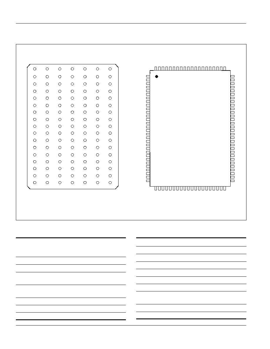
PIN CONFIGURATION
PIN DESCRIPTIONS
A0, A1
Synchronous Address Inputs. These
pins must tied to the two LSBs of the
address bus.
A2-A16
Synchronous Address Inputs
CLK
Synchronous Clock
ADSP
Synchronous Processor Address
Status
ADSC
Synchronous Controller Address
Status
ADV
Synchronous Burst Address Advance
BW1-BW4
Individual Byte Write Enable
BWE
Synchronous Byte Write Enable
GW
Synchronous Global Write Enable
CE, CE2, CE2 Synchronous Chip Enable
OE
Output Enable
DQa-DQd
Synchronous Data Input/Output
MODE
Burst Sequence Mode Selection
V
CC
+3.3V Power Supply
GND
Ground
V
CCQ
Isolated Output Buffer Supply:
+3.3V
ZZ
Snooze Enable
DQPa-DQPd
Parity Data I/O
A
B
C
D
E
F
G
H
J
K
L
M
N
P
R
T
U
VCCQ
NC
NC
DQc1
DQc2
VCCQ
DQc5
DQc7
VCCQ
DQd1
DQd4
VCCQ
DQd6
DQd8
NC
NC
VCCQ
A6
CE2
A7
DQPc
DQc3
DQc4
DQc6
DQc8
VCC
DQd2
DQd3
DQd5
DQd7
DQPd
A5
NC
NC
A4
A3
A2
GND
GND
GND
BW3
GND
NC
GND
BW4
GND
GND
GND
MODE
A10
NC
ADSP
ADSC
VCC
NC
CE
OE
ADV
GW
VCC
CLK
NC
BWE
A1
A0
VCC
A11
NC
A8
A9
A12
GND
GND
GND
BW2
GND
NC
GND
BW1
GND
GND
GND
GND
A14
NC
A16
CE2
A15
DQPb
DQb6
DQb5
DQb4
DQb2
VCC
DQa7
DQa5
DQa4
DQa3
DQPa
A13
NC
NC
VCCQ
NC
NC
DQb8
DQb7
VCCQ
DQb3
DQb1
VCCQ
DQa8
DQa6
VCCQ
DQa2
DQa1
NC
ZZ
VCCQ
1 2 3 4 5 6 7
DQPb
DQb8
DQb7
VCCQ
GND
DQb6
DQb5
DQb4
DQb3
GND
VCCQ
DQb2
DQb1
GND
NC
VCC
ZZ
DQa8
DQa7
VCCQ
GND
DQa6
DQa5
DQa4
DQa3
GND
VCCQ
DQa2
DQa1
DQPa
A6
A7
CE
CE2
BW4
BW3
BW2
BW1
CE2
VCC
GND
CLK
GW
BWE
OE
ADSC
ADSP
ADV
A8
A9
DQPc
DQc1
DQc2
VCCQ
GND
DQc3
DQc4
DQc5
DQc6
GND
VCCQ
DQc7
DQc8
NC
VCC
NC
GND
DQd1
DQd2
VCCQ
GND
DQd3
DQd4
DQd5
DQd6
GND
VCCQ
DQd7
DQd8
DQPd
1
2
3
4
5
6
7
8
9
10
11
12
13
14
15
16
17
18
19
20
21
22
23
24
25
26
27
28
29
30
80
79
78
77
76
75
74
73
72
71
70
69
68
67
66
65
64
63
62
61
60
59
58
57
56
55
54
53
52
51
100 99 98 97 96 95 94 93 92 91 90 89 88 87 86 85 84 83 82 81
31 32 33 34 35 36 37 38 39 40 41 42 43 44 45
MODE
A5
A4
A3
A2
A1
A0
NC
NC
GND
VCC
NC
NC
A10
A11
A12
A13
A14
A15
A16
46 47 48 49 50
128K x 36
119-pin PBGA (Top View)
100-Pin TQFP

IS61SF12832
IS61SF12836
ISSI
®
Integrated Silicon Solution, Inc. -- 1-800-379-4774
5
Rev. A
04/17/01
TRUTH TABLE
Address
Operation
Used
CE
CE2
CE2
ADSP ADSC
ADV WRITE
OE
DQ
Deselected, Power-down
None
H
X
X
X
L
X
X
X
High-Z
Deselected, Power-down
None
L
X
H
L
X
X
X
X
High-Z
Deselected, Power-down
None
L
L
X
L
X
X
X
X
High-Z
Deselected, Power-down
None
X
X
H
H
L
X
X
X
High-Z
Deselected, Power-down
None
X
L
X
H
L
X
X
X
High-Z
Read Cycle, Begin Burst
External
L
H
L
L
X
X
X
X
Q
Read Cycle, Begin Burst
External
L
H
L
H
L
X
Read
X
Q
Write Cycle, Begin Burst
External
L
H
L
H
L
X
Write
X
D
Read Cycle, Continue Burst
Next
X
X
X
H
H
L
Read
L
Q
Read Cycle, Continue Burst
Next
X
X
X
H
H
L
Read
H
High-Z
Read Cycle, Continue Burst
Next
H
X
X
X
H
L
Read
L
Q
Read Cycle, Continue Burst
Next
H
X
X
X
H
L
Read
H
High-Z
Write Cycle, Continue Burst
Next
X
X
X
H
H
L
Write
X
D
Write Cycle, Continue Burst
Next
H
X
X
X
H
L
Write
X
D
Read Cycle, Suspend Burst
Current
X
X
X
H
H
H
Read
L
Q
Read Cycle, Suspend Burst
Current
X
X
X
H
H
H
Read
H
High-Z
Read Cycle, Suspend Burst
Current
H
X
X
X
H
H
Read
L
Q
Read Cycle, Suspend Burst
Current
H
X
X
X
H
H
Read
H
High-Z
Write Cycle, Suspend Burst
Current
X
X
X
H
H
H
Write
X
D
Write Cycle, Suspend Burst
Current
H
X
X
X
H
H
Write
X
D
PARTIAL TRUTH TABLE
Function
GW
BWE
BW1
BW2
BW3
BW4
Read
H
H
X
X
X
X
Read
H
L
H
H
H
H
Write Byte 1
H
L
L
H
H
H
Write All Bytes
H
L
L
L
L
L
Write All Bytes
L
X
X
X
X
X