IXYS reserves the right to change limits, conditions and dimensions.
CS 29
© 2003 IXYS All rights reserved
Symbol
Conditions
Maximum Ratings
I
T(RMS)
T
VJ
= T
VJM
35
A
I
T(AV)M
T
C
= 95∞C; 180∞ sine (I
T(RMS)
current limit)
23
A
I
TSM
T
VJ
= 45∞C;
t = 10 ms (50 Hz), sine
200
A
V
R
= 0 V
t = 8.3 ms (60 Hz), sine
215
A
T
VJ
= T
VJM
;
t = 10 ms (50 Hz), sine
175
A
V
R
= 0 V
t = 8.3 ms (60 Hz), sine
185
A
I
2
t
T
VJ
= 45∞C;
t = 10 ms (50 Hz), sine
200
A
2
s
V
R
= 0 V
t = 8.3 ms (60 Hz), sine
195
A
2
s
T
VJ
= T
VJM
;
t = 10 ms (50 Hz), sine
155
A
2
s
V
R
= 0 V
t = 8.3 ms (60 Hz), sine
145
A
2
s
(di/dt)
cr
T
VJ
= T
VJM
;
repetitive, I
T
= 40 A
150
A/µs
f = 50 Hz; t
P
= 200 µs;
V
D
=
2
/
3
V
DRM
;
I
G
= 0.2 A;
non repetitive, I
T
= I
T(AV)M
500
A/µs
di
G
/dt = 0.2 A/µs
(dv/dt)
cr
T
VJ
= T
VJM
;
V
DR
=
2
/
3
V
DRM
;
1000
V/µs
R
GK
=
; method 1 (linear voltage rise)
P
GM
T
VJ
= T
VJM
;
t
P
= 30 µs
5
W
I
T
= I
T(AV)M
;
t
P
= 300 µs
2.5
W
P
GAV
0.5
W
V
RGM
10
V
T
VJ
-40...+150
∞C
T
VJM
150
∞C
T
stg
-40...+150
∞C
V
ISOL
50/60 Hz RMS; I
ISOL
1 mA
2500
V~
T
L
1.6 mm from case; 10 s
260
∞C
F
C
Mounting force
11...65 / 2.4...11
N/lb
Weight
2
g
V
RRM
= 800/1200 V
I
T(RMS)
= 35 A
I
T(AV)M
= 23 A
V
RSM
V
RRM
Type
V
DSM
V
DRM
V
V
800
800
CS 29-08io1C
1200
1200
CS 29-12io1C
Features
∑
Silicon chip on Direct-Copper-Bond
substrate
- High power dissipation
- Isolated mounting surface
- 2500 V electrical isolation
∑
Low cathode-to-tab capacitance
(15 pF typical)
∑
Planar passivated chips
∑
Epoxy meets UL 94V-0
∑
High performance glass passivated chip
∑
Long-term stability of leakage
current and blocking voltage
Applications
∑
Motor control
∑
Power converter
∑
AC power controller
∑
Light and temperature control
∑
SCR for inrush current limiting
in power supplies or AC drive
Advantages
∑
Space and weight savings
∑
Simple mounting
98839A (04/28)
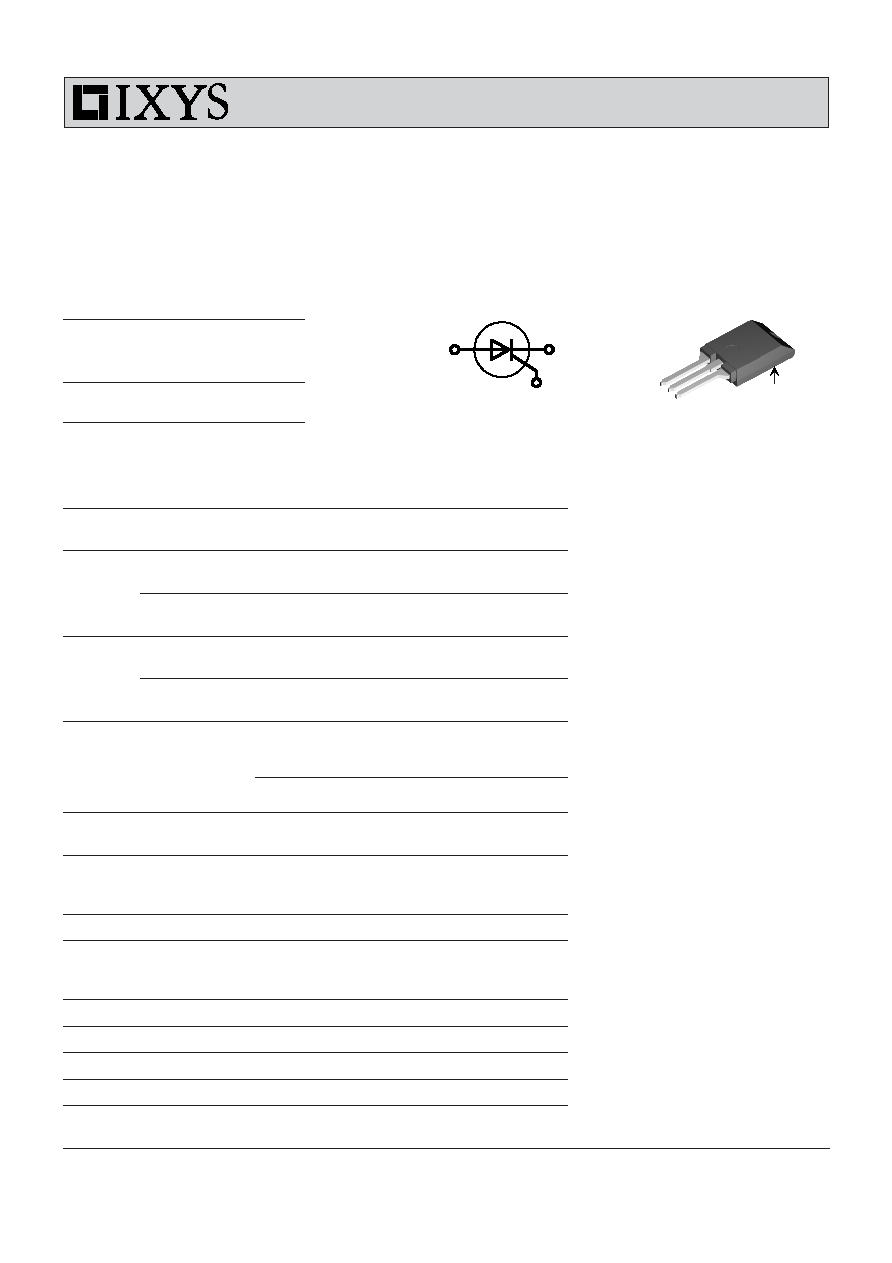
Phase Control Thyristor
ISOPLUS220
TM
Electrically Isolated Back Surface
Preliminary Data Sheet
A
C
G
* Patent pending
1
2
3
Isolated back surface*
ISOPLUS220
TM
CS 29
© 2003 IXYS All rights reserved
Symbol
Conditions
Characteristic Values
I
R
, I
D
T
VJ
= T
VJM
; V
R
= V
RRM
; V
D
= V
DRM
2
mA
V
T
I
T
= 45 A; T
VJ
= 25∞C
1.5
V
V
T0
For power-loss calculations only (T
VJ
= 125∞C)
0.82
V
r
T
16.5
m
V
GT
V
D
= 6 V;
T
VJ
= 25∞C
1.0
V
T
VJ
= -40∞C
1.2
V
I
GT
V
D
= 6 V;
T
VJ
= 25∞C
65
mA
T
VJ
= -40∞C
80
mA
V
GD
T
VJ
= T
VJM
; V
D
=
2
/
3
V
DRM
0.2
V
I
GD
5
mA
I
L
T
VJ
= 25∞C; t
P
= 10 µs;
150
mA
I
G
= 0.2; di
G
/dt = 0.2 A/µs
I
H
T
VJ
= 25∞C; V
D
= 6 V; R
GK
=
50
mA
t
gd
T
VJ
= 25∞C; V
D
= Ω V
DRM
;
2
µs
I
G
= 0.2 A; di
G
/dt = 0.2 A/µs
R
thJC
DC current
1.2
K/W
R
thCK
DC current
typical
0.6
K/W
a
Max. acceleration, 50 Hz
50
m/s
2
See CS 30..io1 data sheet for electrical characteristic curves.
Fig. 1 Gate trigger range
Fig. 2 Gate controlled delay time t
gd
10
100
1000
1
10
100
1000
µ
s
t
gd
I
G
1
10
100
1000
10000
0.1
1
10
I
G
V
G
mA
V
4
2
1
5
6
mA
typ.
Limit
3
I
GD
, T
VJ
=125∞C
1: I
GT
, T
VJ
= 125∞C
2: I
GT
, T
VJ
= 25∞C
3: I
GT
, T
VJ
= -40∞C
4: P
GAV
= 0.5 W
5: P
GM
= 5 W
6: P
GM
= 10 W
T
VJ
= 25∞C
ISOPLUS220 OUTLINE
Note: All terminals are solder plated.
1 - Cathode
2 - Anode
3 - Gate
IXYS reserves the right to change limits, conditions and dimensions.
CS 29
© 2003 IXYS All rights reserved
0
20
40
60
80
100 120
0
10
20
30
40
50
60
70
80
I
T(AV)M
0
10
20
30
40
50
60
70
0
20
40
60
80
100
120
140
0
25
50
75
100
125
150
0.001
0.01
0.1
1
0
100
200
300
400
0.0
0.5
1.0
1.5
2.0
0
20
40
60
80
100
I
TSM
I
T
A
V
T
t
s
P
T
W
I
T(AV)M
A
T
amb
∞C
V
A
1
2
3
4
5 6 7 8 910
1000
I
2
t
t
A
2
s
T
case
A
∞C
ms
500
2000
Fig. 3
Forward characteristics
Fig. 4 Surge overload current
I
TSM
: crest value, t: duration
Fig. 5 I
2
t versus time (1-10 ms)
Fig. 6
Power dissipation versus forward current and ambient temperature
T
VJ
= 125∞C
T
VJ
= 45∞C
50Hz, 80%V
RRM
T
VJ
= 125∞C
DC
180∞ sin
120∞
60∞
30∞
R
thKA
:
0.1 K/W
0.5 K/W
1 K/W
2 K/W
4 K/W
10 K/W
T
VJ
= 45∞C
DC
180∞ sin
120∞
60∞
30∞
V
R
= 0 V
T
VJ
= 25∞C
T
VJ
= 125∞C