© 2004 IXYS All rights reserved
1 - 2
DSEP 6-06AS
432
IXYS reserves the right to change limits, test conditions and dimensions.
HiPerFRED
TM
Epitaxial Diode
with soft recovery
Features
∑ Planar passivated chips
∑ Very short recovery time
∑ Extremely low switching losses
∑ Low I
RM
-values
∑ Soft recovery behaviour
Applications
∑ Anti saturation diode
∑ Snubber diode
∑ Free wheeling diode in converters
and motor control circuits
∑ Rectifiers in switch mode power
supplies (SMPS)
∑ Inductive heating and melting
∑ Uninterruptible power supplies (UPS)
∑ Ultrasonic cleaners and welders
Advantages
∑ High reliability circuit operation
∑ Low voltage peaks for reduced
protection circuits
∑ Low noise switching
∑ Low losses
∑ Operating at lower temperature or
space saving by reduced cooling
Dimensions see pages D4 - 85-86
I
FAVM
= 6 A
V
RRM
= 600 V
t
rr
= 20 ns
TO-252AA (DPAK)
Anode
Anode
Cathode (Flange)
V
RSM
V
RRM
Type
Marking
V
V
on product
600
600
DSEP 6-06AS
6P060AS
C
A
Symbol
Conditions
Maximum Ratings
I
FRMS
T
VJ
= T
VJM
26
A
I
FAVM
T
C
= 152∞C; rectangular, d = 0.5
6
A
I
FRM
t
P
< 10 µs; rep. rating, pulse width limited by T
VJM
12
A
I
FSM
T
VJ
= 45∞C; t = 10 ms
(50 Hz), sine
40
A
E
AS
T
VJ
= 25∞C; non-repetitive
0.1
mJ
I
AS
= 0.8 A; L = 180 µH
I
AR
V
A
= 1.5∑V
R
typ.; f = 10 kHz; repetitive
0.1
A
T
VJ
-40...+175
∞C
T
VJM
175
∞C
T
stg
-40...+150
∞C
P
tot
T
C
= 25∞C
55
W
Weight
typ.
0.3
g
I
FAVM
rating includes reverse blocking losses
at T
VJM
, V
R
= 0.6 V
RRM
, duty cycle d = 0.5
Data according to IEC 60747
Symbol
Conditions
Characteristic Values
typ.
max.
I
R
T
VJ
= 25∞C
V
R
= V
RRM
50
µA
T
VJ
= 150∞C V
R
= V
RRM
0.2
mA
V
F
I
F
= 6 A;
T
VJ
= 150∞C
1.33
V
T
VJ
= 25∞C
2.02
V
R
thJC
2.8
K/W
t
rr
I
F
= 1 A; -di/dt = 200 A/µs; V
R
= 30 V; T
VJ
= 25∞C
20
tbd
ns
I
RM
V
R
= 100 V; I
F
= 10 A; -di
F
/dt = 100 A/µs
3.5
4.4
A
T
VJ
= 100∞C
© 2004 IXYS All rights reserved
2 - 2
DSEP 6-06AS
432
IXYS reserves the right to change limits, test conditions and dimensions.
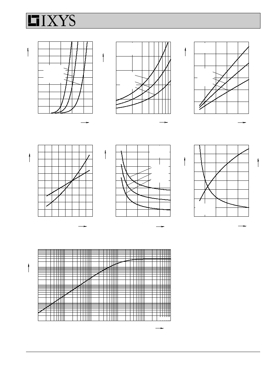
NOTE: Fig. 2 to Fig. 6 shows typical values
200
600
1000
0
400
800
60
70
80
90
100
110
0.00001
0.0001
0.001
0.01
0.1
1
0.001
0.01
0.1
1
10
0
40
80
120
160
0.0
0.4
0.8
1.2
1.6
2.0
K
f
T
VJ
∞C
-di
F
/dt
t
s
K/W
0
200
400
600
800
1000
0
5
10
15
20
0.0
0.3
0.6
0.9
1.2
V
FR
di
F
/dt
V
200
600
1000
0
400
800
0
10
20
30
100
1000
0
200
400
600
800
1000
0.0
0.5
1.0
1.5
2.0
0
2
4
6
8
10
I
RM
Q
r
I
F
A
V
F
-di
F
/dt
-di
F
/dt
A/
µs
A
V
nC
A/
µs
A/
µs
t
rr
ns
t
fr
A/
µs
µs
DSEP 6-06AS
Z
thJC
T
VJ
=150∞C
T
VJ
=100∞C
T
VJ
= 25∞C
I
F
= 12A
I
F
= 6A
I
F
= 3A
T
VJ
= 100∞C
V
R
= 300V
T
VJ
= 100∞C
V
R
= 300V
T
VJ
= 100∞C
V
R
= 300V
T
VJ
= 100∞C
I
F
= 6A
V
FR
t
fr
I
RM
Q
r
I
F
= 12A
I
F
= 6A
I
F
= 3A
I
F
= 12A
I
F
= 6A
I
F
= 3A
Fig. 3 Peak reverse current I
RM
versus -di
F
/dt
Fig. 2 Reverse recovery charge Q
r
versus -di
F
/dt
Fig. 1 Forward current I
F
versus V
F
Fig. 4 Dynamic parameters Q
r
, I
RM
versus T
VJ
Fig. 5 Recovery time t
rr
versus -di
F
/dt
Fig. 6 Peak forward voltage V
FR
and t
fr
versus di
F
/dt
Fig. 7 Transient thermal resistance junction to case