© 2000 IXYS All rights reserved
1 - 2
Pulse test:
Pulse Width = 5 ms, Duty Cycle < 2.0 %
Data according to IEC 60747 and per diode unless otherwise specified
IXYS reserves the right to change limits, Conditions and dimensions.
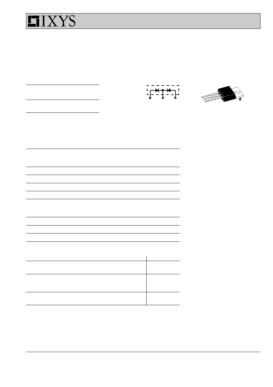
Power Schottky Rectifier
with common cathode
A
C
A
TO-220 AB
C (TAB)
A
C
A
A = Anode, C = Cathode , TAB = Cathode
Features
∑ International standard package
∑ Very low V
F
∑ Extremely low switching losses
∑ Low I
RM
-values
∑ Epoxy meets UL 94V-0
Applications
∑ Rectifiers in switch mode power
supplies (SMPS)
∑ Free wheeling diode in low voltage
converters
Advantages
∑ High reliability circuit operation
∑ Low voltage peaks for reduced
protection circuits
∑ Low noise switching
∑ Low losses
Dimensions see outlines.pdf
Symbol
Conditions
Maximum Ratings
I
FRMS
35
A
I
FAV
T
C
= 165
∞
C; rectangular, d = 0.5
10
A
I
FAV
T
C
= 165
∞
C; rectangular, d = 0.5; per device
20
A
I
FSM
T
VJ
= 45∞C; t
p
= 10 ms (50 Hz), sine
200
A
E
AS
I
AS
= tbd A; L = 180 µH; T
VJ
= 25∞C; non repetitive
tbd
mJ
I
AR
V
A
=1.5 ∑ V
RRM
typ.; f=10 kHz; repetitive
tbd
A
(dv/dt)
cr
18000
V/
m
s
T
VJ
-55...+175
∞
C
T
VJM
175
∞
C
T
stg
-55...+150
∞
C
P
tot
T
C
= 25
∞
C
105
W
M
d
mounting torque
0.4...0.6
Nm
Weight
typical
2
g
I
FAV
= 2x10 A
V
RRM
= 130 V
V
F
= 0.65 V
DSSK 20-013A
DSSK 20-015A
007
V
RSM
V
RRM
Type
V
V
130
130
DSSK 20-013A
150
150
DSSK 20-015A
Symbol
Conditions
Characteristic Values
typ.
max.
I
R
T
VJ
= 25∞C
V
R
= V
RRM
0.5
mA
T
VJ
= 125∞C V
R
= V
RRM
5.0
mA
V
F
I
F
= 10 A;
T
VJ
= 125∞C
0.65
V
I
F
= 10 A;
T
VJ
=
25∞C
0.79
V
I
F
= 20 A;
T
VJ
= 125 ∞C
0.72
V
R
thJC
1.4
K/W
R
thCH
0.5
K/W
Preliminary Data
© 2000 IXYS All rights reserved
2 - 2
0.0
0.2
0.4
0.6
0.8
1.0
1.2
1
10
100
0
50
100
150
0.0001
0.001
0.01
0.1
1
10
5
15
25
0
10
20
30
0
5
10
15
20
25
30
0.0001
0.001
0.01
0.1
1
10
0.01
0.1
1
0
40
80
120
160
0
10
20
30
40
I
F(AV)
T
C
∞C
I
F(AV)
t
s
K/W
10
100
1000
10000
100
1000
10000
I
FSM
t
P
A
0
50
100
150
10
100
1000
C
T
I
R
I
F
A
V
F
V
R
V
R
V
pF
V
mA
A
P
(AV)
W
Z
thJC
V
Single Pulse
DSSK 20-013A
A
µs
T
VJ
=175∞C
150∞C
125∞C
100∞C
50∞C
25∞C
T
VJ
=
175∞C
125∞C
25∞C
T
VJ
= 25∞C
d=0.5
d =
DC
0.5
0.33
0.25
0.17
0.08
75∞C
DC
0.08
D=0.5
0.33
0.25
0.17
2
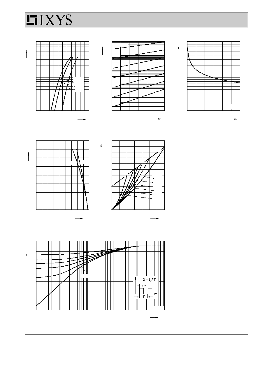
Fig. 3 Typ. junction capacitance C
T
versus reverse voltage V
R
Fig. 2 Typ. value of reverse current I
R
versus reverse voltage V
R
Fig. 1 Maximum forward voltage
drop characteristics
Fig. 4 Average forward current I
F(AV)
versus case temperature T
C
Fig. 5 Forward power loss
characteristics
Fig. 6 Transient thermal impedance junction to case at various duty cycles
DSSK 20-013A
DSSK 20-015A
007