 | –≠–ª–µ–∫—Ç—Ä–æ–Ω–Ω—ã–π –∫–æ–º–ø–æ–Ω–µ–Ω—Ç: IRPLLNR1 | –°–∫–∞—á–∞—Ç—å:  PDF PDF  ZIP ZIP |
Reference Design Data Sheet intended for design information only.
Subjected to changes without prior notice.
1
Reference Design Data Sheet (August, 1997)
IRPLLNR1
POWIRLIGHT
TM
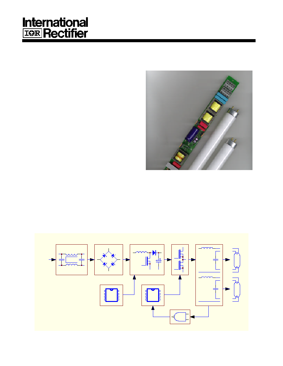
REFERENCE DESIGN : LINEAR BALLAST
Features
∑
Drive 2X40WT12
∑
Universal Input (90-255Vac)
∑
High Power Factor (0.99) & Low THD
∑
High-Frequency Operation (40kHz)
∑
Lamp Filament Preheating
∑
Lamp Fault Protection with Auto-Restart
∑
Over Temperature Protection
∑
IR2153 HVIC Ballast Controller
Description
The IRPLLNR1 is a high efficiency, high
power factor, non-dimmable electronic ballast
designed for linear fluorescent lamp types.
The design contains an active power factor
correction circuit for universal voltage input
and a ballast control circuit using the IR2153
for controlling the lamp. Other features
include EMI filtering, transient protection and
lamp fault protection. The IRPLLNR1 is
intended as a reference design to be used as
development tool to speed up customers'
time to market.
Block Diagram
EMI Filter
Half-Bridge
PFC
Rectifier
Output Stage
Fault Logic
Line
Lamps
IR2153
PFC Control

Reference Design Data Sheet intended for design information only.
Subjected to changes without prior notice.
2
IRPLLNR1
Electrical Characteristics
Parameter
Units
Value
Lamp Type
2/40T12
Input Power
[W]
80 +/- 7%
Input Current (120VAC)
[A]
0.67
Pre-heat Output Frequency
[kHz]
50
Pre-heat Output Voltage
[Vpp]
350
Pre-heat Time
[s]
2.0
Running Output Frequency
[kHz]
39.0 +/- 4%
Running Output Voltage
[V]
100
Input A.C. Voltage Range
[VAC]
90..255VAC/50/60Hz
Input D.C. Voltage Range
[VDC]
100..350
Ambient Temperature Range
[∫C]
0..50
Power Factor
0.99
Total Harmonic Distortion
[%]
<15%
Maximum Output Ignition Voltage
[Vpp]
1200
Note: Other lamp types require a new ballast type with different component values.
Note: Tolerances were achieved with trimming.
Lamp Fault Protection Characteristics
Lamps
Ballast
Restart Operation
Lamp 1 or Lamp 2
lower cathode broken
Deactivates
Lamp exchange or recycle line voltage
Lamp1 or Lamp 2
upper cathode broken
Deactivates if non-
zvs occurs
Exchange damaged lamp or recycle
line voltage
Both Lamps
upper cathodes broken
Deactivates
Lamp exchange or recycle line voltage
Lamp1 or Lamp2
non-strike (cathodes intact)
Deactivates
Lamp exchange or recycle line voltage
Open-Circuit (no lamps)
Deactivates
Lamp exchange or recycle line voltage
Short-Circuit (false hook-up)
Deactivates
Lamp exchange or recycle line voltage

Reference Design Data Sheet intended for design information only.
Subjected to changes without prior notice.
3
IRPLLNR1
Functional Description
Overview
The IRPLLNR1 consists of a power factor front end, a ballast control section, a resonant lamp
output stage and shutdown circuitry. The power factor controller is a boost converter
operating in critically continuous, free-running frequency mode. The ballast control section
provides frequency modulation control of a traditional RCL series-parallel lamp resonant
output circuit and is easily adaptable to a wide variety of lamp types. The shutdown section
consists of lamp circuit current detection and comparator logic for safe turn-off and smooth
auto re-starting. All functional descriptions are referred to the IRPLLNR1 schematic.
Power Factor Control
The power factor controller section consists of the LinFinity LX1562 Power Factor Controller IC
(IC1), MOSFET M1, inductor L3, diode D5, capacitor C8 and additional biasing, sensing and
compensation components (see schematic). This IC was chosen for its minimal component
count, low start-up supply current and robust error amplifier. This is a boost topology designed
to step-up and regulate the output DC bus voltage while drawing sinusoidal input current from
the line (low THD) which is "in phase" with the AC input line voltage (HPF). The charging
current of L3 is sensed in the source of M1 (R7) and the zero-crossing of the inductor current,
as it charges the DC bus capacitor C8, is sensed by a secondary winding on L3. The result is
critically continuous, free-running frequency operation where:
L
V V
V
P V f
in
out
in
out out s
3
2
2
2
=
-
(
)
(1)
I
P
V
L
out
in
p
=
2 2
min
(2)
where,
=
efficiency
V
in
=
nominal AC input voltage
V
out
=
DC bus voltage
P
out
=
lamp power
f
s
=
switching frequency
The value of the boost inductor (L3) can be calculated and the core should be dimensioned to
not saturate at the worst case peak inductor currents (
I
L
p
) for the desired input voltage range.
For universal input, the boost inductor has been dimensioned for the highest peak currents
which occur at low line (90VAC). Because of the wide input voltage range, performance can
vary. It is recommended that the boost inductor be redimensioned for the exact desired input
voltage plus tolerances (+/- 15%).
Reference Design Data Sheet intended for design information only.
Subjected to changes without prior notice.
4
IRPLLNR1
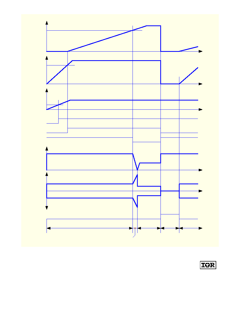
Ballast Control
The ballast control section includes a voltage-controlled oscillator (VCO) (Q1, C20, D9 and
C13) connected to the IR2153 ballast controller IC (IC3) and programmed to different
operating frequencies with a voltage divider (R17, R41, R42, R51, C12). It drives the lamp
resonant output stage (L4, C21 and L5, C23) to the preheat, ignition and running operating
conditions by changing the voltage at the base of Q1 and therefore the frequency of the half-
bridge switches. During preheat, the half-bridge operating frequency is set by R42 and is fixed
for a duration of time determined by the charging time of capacitor C28 to a threshold voltage
(see
Ballast Control Logic and Timing Diagram). This heats the lamp filaments to their
emission temperature before the lamp ignites. This increases the life of the lamp and
decreases ignition voltages and currents, yielding reduced maximum voltage and current
ratings of the lamp resonant output stage and the half-bridge power MOSFETs (M4, M5).
When the voltage on capacitor C28 exceeds the threshold voltage (voltage on C10), R51 is
switched to ground through a comparator of IC4 (pin2) sweeping the voltage on the base of
Q1 to ground momentarily, therefore sweeping the frequency lower towards the resonance
frequency for ignition. The ignition frequency is the minimum frequency of the VCO defined
as,
f
C
R
ignition
=
+
1
113
13
20
75
. (
)(
)
(3)
During the ignition ramp, C12 charges at a much slower rate than C20, resulting in the voltage
at the base of Q1 increasing after ignition to a value determined by the parallel connected
resistor R51. R51 sets the final running frequency where the lamp is driven to the
manufacturer's recommended lamp power rating. The running frequency of the lamp resonant
output stage for selected component values is defined as,
f
LC
P
CV
LC
P
CV
V
V
L C
run
Lamp
Lamp
Lamp
Lamp
DCbus
Lamp
=
-
+
-
-
-
1
2
1
2
1
2
4
1
2
2
2
2
2
2
2
2
2
(4)
where,
L
=
Lamp resonant circuit inductor
[H]
C
=
Lamp resonant circuit capacitor
[F]
P
Lamp
=
Lamp running power
[W]
V
Lamp
=
Lamp running voltage amplitude
[V]

Reference Design Data Sheet intended for design information only.
Subjected to changes without prior notice.
5
IRPLLNR1
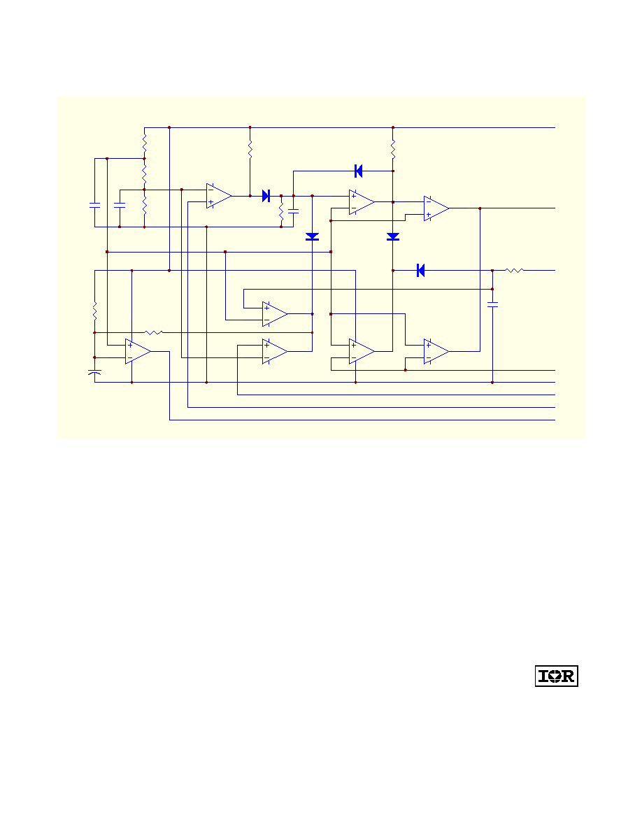
Fault Protection
The shutdown circuitry consists of 2 quad comparator ICs (IC2 and IC4), a current detection
filter (R21, R22, C16 and D12), a pull-up lamp removal circuit (R23, R24, R25, R26, D16 and
C22), and over-current sensing resistors (R47, R48, R49, R43, R44, R46, D10 and D19). A
more detailed diagram of the logic circuitry is given in the
Ballast Control Logic and Timing
sections of this paper. The current detection filter rectifies and integrates a measurement of
the lamp resonant current from the source of the lower MOSFET of the half-bridge and
compares it against a fixed threshold voltage. Should the current exceed the threshold in the
event of over-current due to a non-strike condition of the lamp or non-zero voltage switching of
the half-bridge due to an open circuit or broken lamp cathodes, the CT pin of the IR2153 is
latched below the internal shutdown threshold (1/6 Vcc) and the ballast is shutdown.
In the event of a lamp exchange, the latch is reset with the pull-up network at the lamp,
and the CT pin of the IR2153 is held below the internal shutdown threshold in an
unlatched
state (see
Timing Diagram). When a new lamp is re-inserted, the ballast performs an auto
restart without a recycling of the input line voltage. During a lamp removal, the frequency is
also reset to the preheat frequency to avoid damage to the half-bridge switches due to below-
resonance operation which can occur upon re-insertion of the lamp. For a dual lamp ballast, a
second pull-up network is added to the second lamp (R27, R28, R29, R30) and is `OR-ed'
together with the first lamp. If either lamp is removed during running, the ballast is shutdown.
In the event of a broken
upper cathode by either lamp during normal operation, non zero-
voltage switching occurs at the half-bridge and will be detected by the current detection filter at
source of the lower MOSFET of the half-bridge. Both half-bridge MOSFETs are latched off.
Should the DC bus decrease below a fixed threshold voltage during an undervoltage
condition of the line voltage, the frequency is shifted back up to the preheat frequency to fulfill
zero-voltage switching of the half-bridge, and the latch is disabled. This prevents latch-up
during a fast cycling of the line voltage or a brown out.
IRPLLNR1

Reference Design Data Sheet intended for design information only.
Subjected to changes without prior notice.
6
Trimming
The final ballast running input power during production can vary due to tolerances in L, C,
VBUS, frun and manufacturing of the lamp. Trimming is therefore recommended. An
insulated jumper wire (JP1) is connected over resistor R50 to accommodate for this. If the
final run frequency exceeds the nominal specified run frequency by 4% (39kHz), the input
power will be too low, and the ballast may not ignite the lamp and/or deactivate in the event of
a non-strike condition. This is because RT (R20) programs the minimum operating frequency
which corresponds to the ignition frequency. If this frequency is too high, the resulting lamp
voltage may be too low to ignite the lamp and the resulting current may be too low to reach the
current limit threshold. Shifting this frequency up or down shifts all other operating frequencies
in the same direction. In this case, JP1 should be cut in two places and removed. This will
connect R50 in series with R20 and decrease all operating frequencies slightly. The running
lamp power, ignition voltage and ignition current will also increase. All of these parameters
should be carefully tested during production.
IRPLLNR1
Ballast Control Logic
For corresponding signal waveforms, see
Timing Diagram.
Reference Design Data Sheet intended for design information only.
Subjected to changes without prior notice.
7
5
4
2
3
12
IC2A
7
6
1
IC2B
9
8
14
IC2C
11
10
13
IC2D
5
4
2
3
12
IC4A
7
6
1
IC4B
9
8
14
IC4C
11
10
13
IC4D
R36
R15
R14
C26
C10
D6
R16
R19
C24
C15
D7
D8
D15
D20
R39
R35
R18
R45
+
C28
VCC
CT(IR2153)
RT(IR2153)
COM
LAMPOUT
OVER-CURRENT
PREHEAT
TBLANK
VTH1
VTH2
UNDERVOLTAGE
FREQSHIFT
RESET
LATCH
SHUTDOWN
(NON-LATCHED)
SHUTDOWN
(LATCHED)
ENABLE
TPHEAT
IRPLLNR1
Timing Diagram (Normal operation, lamp removal/re-insertion during running)
Reference Design Data Sheet intended for design information only.
Subjected to changes without prior notice.
8
VTH1
VTH1
TPHEAT
TBLANK
ENABLE
PREHEAT
V(R41)
I(L4)
LAMPOUT
t
t
t
t
PREHEAT
RUN
SHUTDOWN
PREHEAT
IGN
VTH2
UNDER-
t
FREQSHIFT
VOLTAGE
IRPLLNR1
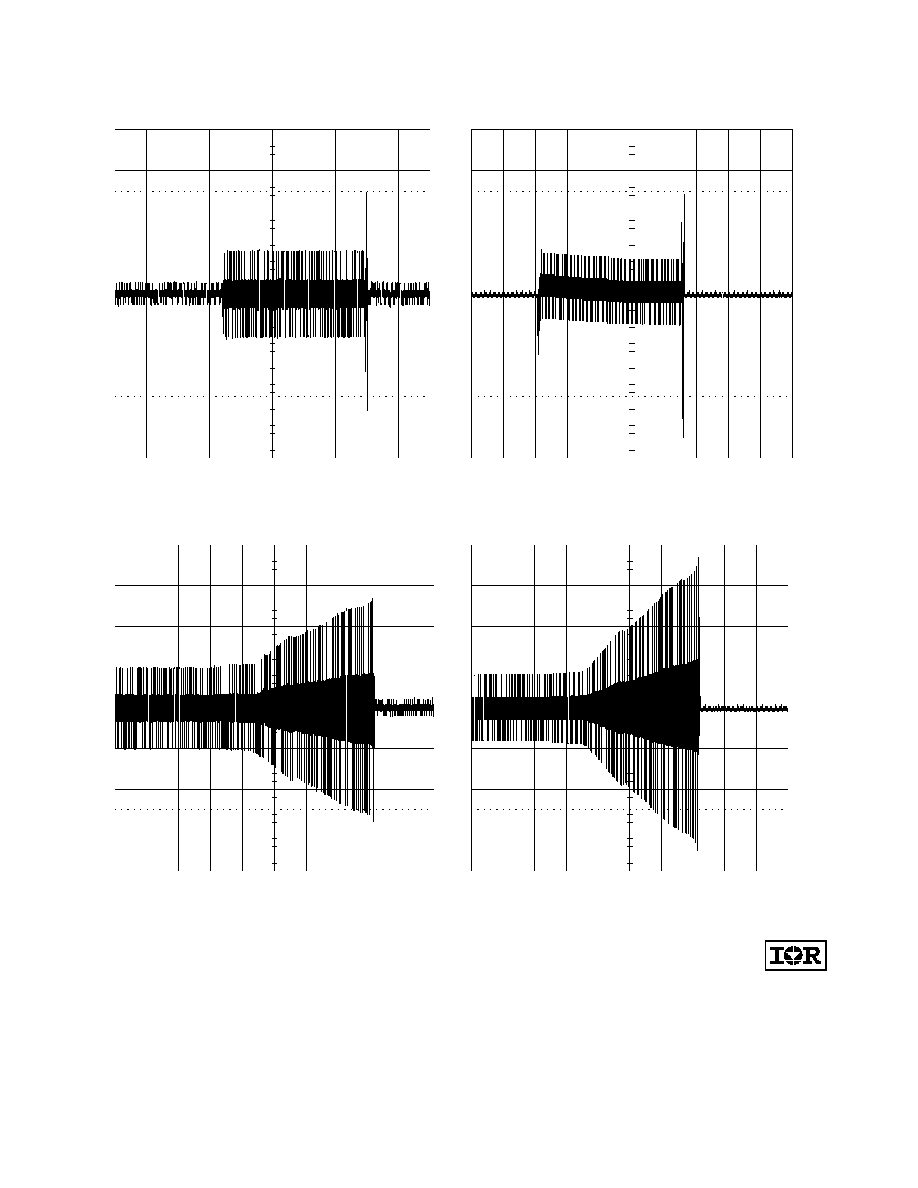
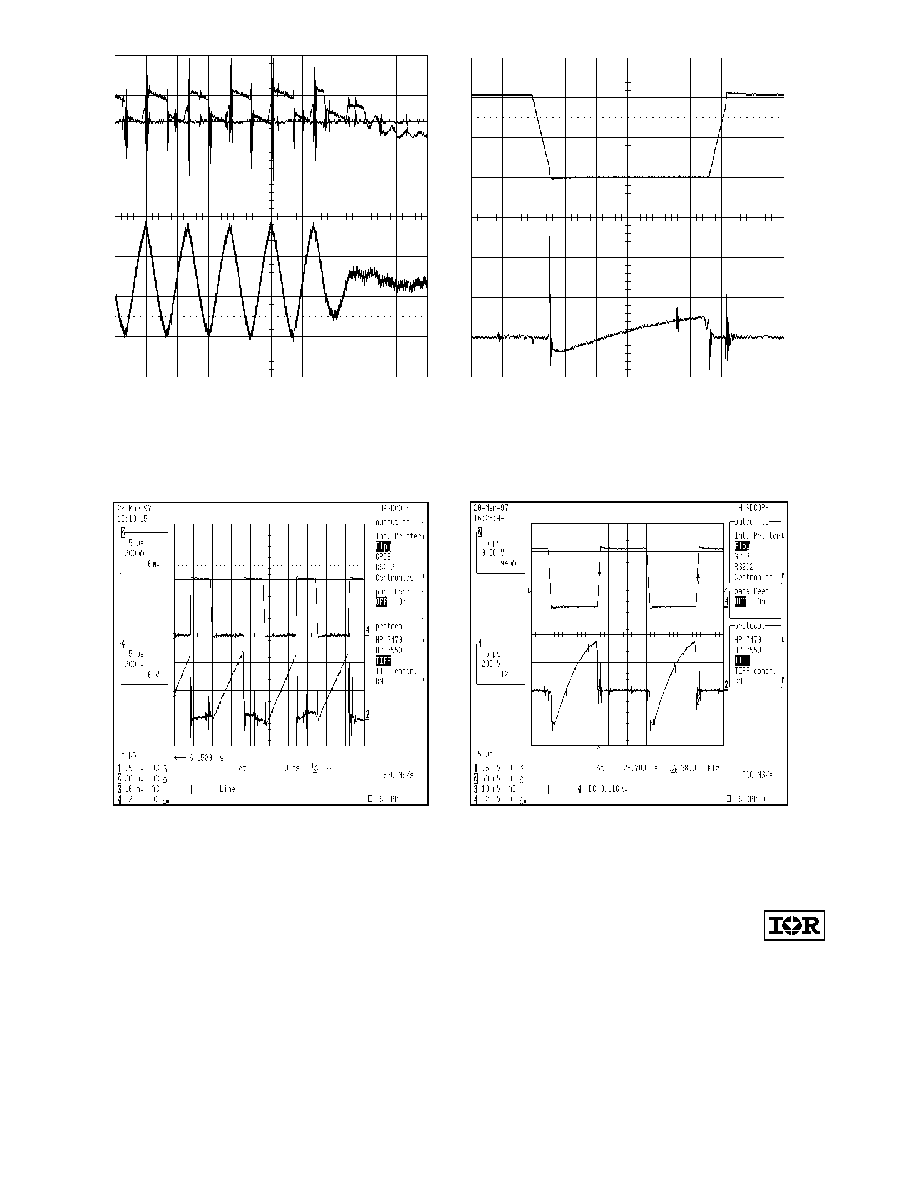
Measurements

Reference Design Data Sheet intended for design information only.
Subjected to changes without prior notice.
9
The following waveforms (see Figures 1 and 2) are from a dual 40W/T12 ballast (see Bill of
Materials) and include ballast input, ouput and control measurements during all modes of
operation.
Figure 1 : Line input voltage (upper trace, 200V/div) and
Figure 2 : Drain-to-source voltage (upper trace, 200V/div)
current (lower trace, 0.5A/div) during 120VAC normal
current (lower trace, 0.5A/div) during 230VAC normal
operation. Timescale = 5ms/div.
operation. Timescale = 5ms/div.
Figure 3 : Line input current (200V/div) during preheat,
Figure 4 : Rectifier output voltage (upper trace, 200V/div),
ignition and running operating conditions.
VCC IR2153 (middle trace, 10V/div) and VDD LX1562
Timescale = 0.5s/div.
(lower trace, 10V/div) during start-up. Timescale = 5ms/div.
IRPLLNR1
Measurements (cont.)
Reference Design Data Sheet intended for design information only.
Subjected to changes without prior notice.
10
Figure 5: Inductor (L4 or L5) current (0.5A/div) during
Figure 6: Lamp voltage (200V/div) during preheat and
preheat and ignition operating conditions.
ignition operating conditions. Timescale = 0.5A/div.
Timescale = 0.5A/div.
Figure 7: Inductor current (L4 or L5) (0.5A/div) ramping up
Figure 8: Lamp voltage (200V/div) ramping up after
after preheat to ignite the lamp. Timescale = 5ms/div.
preheat to ignite the lamp. Timescale = 5ms/div. Dummy
Dummy filaments inserted to simulate non-strike condition.
filaments inserted to simulate non-strike condition.
IRPLLNR1
Measurements (cont.)

Reference Design Data Sheet intended for design information only.
Subjected to changes without prior notice.
11
Figure 9: Filament current (upper trace, 0.5A/div) and
Figure 10: VCO voltage (5V/div) showing control sequence
voltage (lower trace, 10V/div) during preheat.
during preheat, ignition and running conditions.
Timescale = 0.5A/div.
Timescale = 0.5A/div.
Figure 11: Half-bridge voltage (upper trace, 200V/div),
Figure 12: Half-bridge voltage (upper trace, 200V/div)
half-bridge current (middle/upper trace, 1A/div), Vth2
and lampout signal V:D16 (lower trace, 5V/div) during
threshold voltage (middle/lower trace, 1V/div) and current
lamp removal/re-insertion condition. Timescale = 10ms/div.
detection voltage (lower trace, 1V/div) During normal
running condtions. Timescale = 5us/div.
IRPLLNR1
Measurements (cont.)
Reference Design Data Sheet intended for design information only.
Subjected to changes without prior notice.
12
Figure 13: Vth2 threshold voltage (upper middle trace,
Figure 14: Half-bridge voltage (upper trace, 200V/div) and
1V/div), current detection signal V:C16 (upper trace, 1V/div)
lower half-bridge MOSFET source current (1A/div) during
and inductor current (lower trace, 0.5A/div) during non-strike/
hard-switching fault condition. Timescale = 1us/div. Upper
shutdown condition. Timescale = 20us/div. V:C16 exceeds
filament of 1 lamp removed, other lamp remains running.
Vth2 as current ramps up and ballast is shutdown. Dummy
Condition continues until V:C16 exceeds Vth2 (V:C26).
filaments inserted to simulate non-strke condtion.
Figure 15: Voltage (upper trace, 200V/div) and current
Figure 16: Drain-to-source voltage (upper trace, 200V/div)
(lower trace, 0.5A/div) waveforms of PFC MOSFET (M1)
and source current (lower trace, 0.7A/div) of MOSFET (M5)
during lowest line (100VAC) condition.
during maximum running lamp power.
IRPLLNR1
Measurements (cont.)

Reference Design Data Sheet intended for design information only.
Subjected to changes without prior notice.
13
Figure 17: Typical Conducted EMI frequency response for phase against
neutral (upper trace: Quasi Peak, lower trace: Average). EN55015 limit
lines also shown.
Figure 18: Typical Conducted EMI frequency response for neutral against
neutral (upper trace: Quasi Peak, lower trace: Average). EN55015 limit
lines also shown.
Reference Design Data Sheet intended for design information only.
Subjected to changes without prior notice.
14
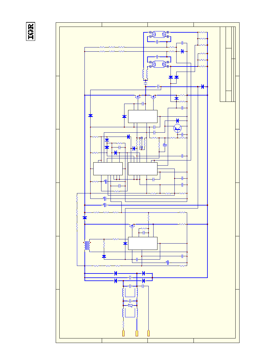
IRPLLNR1
Circuit Schematic
1
2
3
4
5
6
A
B
C
D
6
5
4
3
2
1
D
C
B
A
Title
Number
Revision
Size
B
Date:
8-Jan-1998
Sheet of
File:
C:\PROTEL\SCH\IRPLLNR1\IRPLLNR1.SCH Drawn By:
N
L
R1
R5
5
8
C6
6
3
7
2
R6
1
4
LX1562M
R8
D5
R9
R13
D11
C14
C18
C17
D13
M4
M5
D1
D2
D3
D4
C2
C3
C1
L2
RV1
C19
L4
L5
C23
C21
LP1
LP2
VCC
RT
CT
VB
HO
VS
LO
VSS
IR2153
1 of 1
WARM-START UNIVERSAL INPUT FLUORESCENT BALLAST
R50
R14
R15
R4
R12
R7
M1
C7
C13
C12
C8
R23
R27
R26
R30
D19
D14
D16
L1
L3
C5
C9
C10
R22
R21
C16
R17
F1
400VDC
90..275VAC
Note: Thick traces represent high-frequency, high-current paths. Lead lengths should be minimized to avoid high-frequency noise problems.
C11
R10
R11
R2
R3
R25
R24
R28
R29
C4
50/60Hz
IC1
IC3
3
11
12
TLC339
IC2
1
8
13
4
6
D18
C22
R40
R37
R36
154..254VDC
X2:1
X2:2
X2:3
X2:4
X3:1
X3:3
X3:2
X3:4
D10
R46
R43
R44
R47
R48
R49
3
12
14
1
D8
2
R18
C15
C24
R16
R35
D9
Q1
C20
R42
R41
R19
R39
11
5
7
10
6
5
9
10
R45
2
8
13
C26
TLC339
IC4
9
4
14
X1:1
X1:2
X1:3
E
C27
7
C25
D7
D6
D12
D20
D15
R34
D17
R20
JP1
C28
R51

Reference Design Data Sheet intended for design information only.
Subjected to changes without prior notice.
15
WORLD HEADQUARTERS: 233 KANSAS ST., EL SEGUNDO, CA 90245 USA ∑ (310)322-3331 ∑ FAX (310)322-3332 ∑ TELEX 472-0403
EUROPEAN HEADQUARTERS: HURST GREEN, OXTED, SURREY RH8 9BB, UK ∑ (44)0883 713215 ∑ FAX (944)0883 714234 ∑ TELEX 95219
Sales Offices, Agents and Distributors in Major Cities Throughout the World.
Data and specifications subject to change without notice.
© 1997 International Rectifier Printed in U.S.A. 4-97