© 2003 IXYS All rights reserved
Symbol
Test Conditions
Maximum Ratings
V
DSS
T
J
= 25
∞
C to 150
∞
C
600
V
V
DGR
T
J
= 25
∞
C to 150
∞
C; R
GS
= 1 M
600
V
V
GS
Continuous
±
30
V
V
GSM
Transient
±
40
V
I
D25
T
C
= 25
∞
C
70
A
I
DM
T
C
= 25
∞
C, pulse width limited by T
JM
280
A
I
AR
T
C
= 25
∞
C
70
A
E
AR
T
C
= 25
∞
C
60
mJ
E
AS
T
C
= 25
∞
C
5.0
J
dv/dt
I
S
I
DM
, di/dt
100 A/
µ
s, V
DD
V
DSS
20
V/ns
T
J
150
∞
C, R
G
= 2
P
D
T
C
= 25
∞
C
890
W
T
J
-55 ... +150
∞
C
T
JM
150
∞
C
T
stg
-55 ... +150
∞
C
T
L
1.6 mm (0.063 in.) from case for 10 s
300
∞
C
Symbol
Test Conditions
Characteristic Values
(T
J
= 25
∞
C, unless otherwise specified)
min.
typ. max.
V
DSS
V
GS
= 0 V, I
D
= 1mA
600
V
V
GS(th)
V
DS
= V
GS
, I
D
= 8mA
3.0
5.0
V
I
GSS
V
GS
=
±
30 V, V
DS
= 0
±
200 nA
I
DSS
V
DS
= V
DSS
T
J
= 25
∞
C
50
µ
A
V
GS
= 0 V
T
J
= 125
∞
C
3 mA
R
DS(on)
V
GS
= 10 V, I
D
= 0.5 ∑ I
D25
80 m
Note 1
DS99006(02/03)
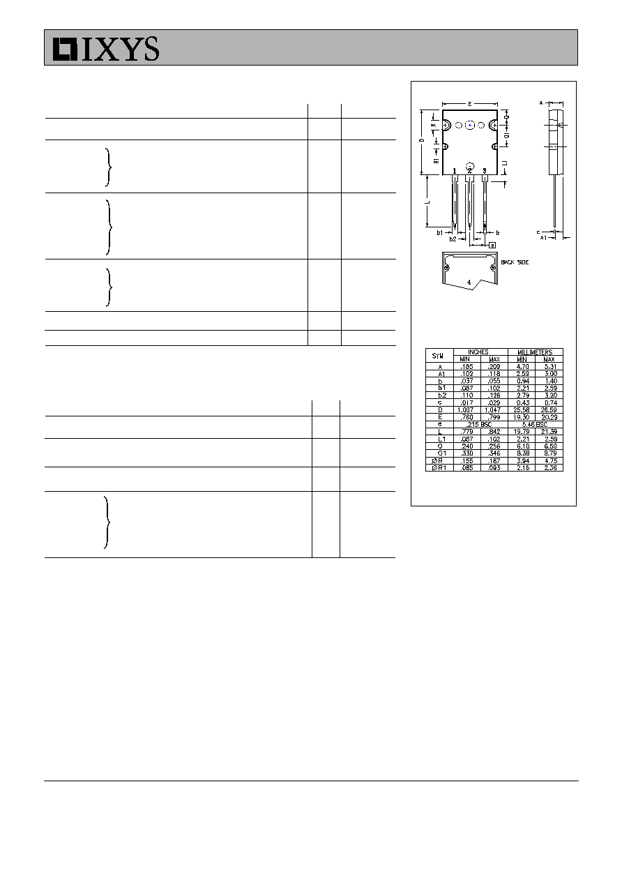
PLUS 264
TM
(IXFB)
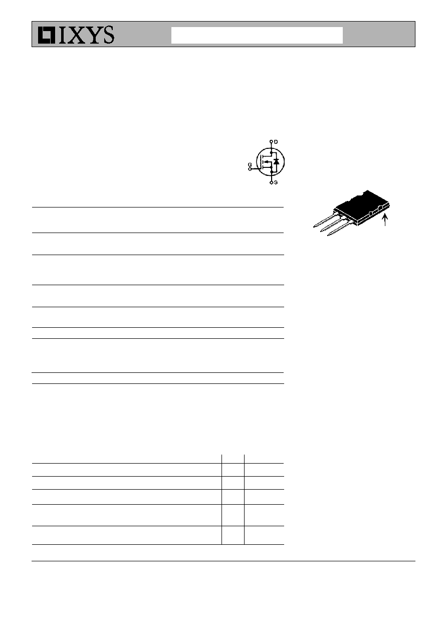
G = Gate
D = Drain
S = Source
TAB = Drain
S
G
D
(TAB)
HiPerFET
TM
Power MOSFETs
Q-Class
N-Channel Enhancement Mode
Avalanche Rated, Low Q
g
,
Low Intrinsic R
g
High dV/dt, Low t
rr
Features
Double metal process for low gate
resistance
Unclamped Inductive Switching (UIS)
rated
Low package inductance
- easy to drive and to protect
Fast intrinsic rectifier
Applications
DC-DC converters
Switched-mode and resonant-mode
power supplies, >500kHz switching
DC choppers
Pulse generation
Laser drivers
Advantages
PLUS 264
TM
package for clip or spring
mounting
Space savings
High power density
IXFB 70N60Q2
V
DSS
= 600 V
I
D25
= 70 A
R
DS(on)
= 80 m
t
rr
250 ns
Advance Technical Information
IXYS reserves the right to change limits, test conditions, and dimensions.
IXYS MOSFETS and IGBTs are covered by one or more of the following U.S. patents:
4,835,592
4,881,106
5,017,508
5,049,961
5,187,117
5,486,715 6,306,728B1
4,850,072
4,931,844
5,034,796
5,063,307
5,237,481
5,381,025
IXFB70N60Q2
Symbol
Test Conditions
Characteristic Values
(T
J
= 25
∞
C, unless otherwise specified)
min.
typ. max.
g
fs
V
DS
= 10 V; I
D
= 0.5 ∑ I
D25
Note 1
36
50
S
C
iss
7200
pF
C
oss
V
GS
= 0 V, V
DS
= 25 V, f = 1 MHz
1300
pF
C
rss
290
pF
t
d(on)
26
ns
t
r
V
GS
= 10 V, V
DS
= 0.5 ∑ V
DSS
, I
D
= 0.5 ∑ I
D25
25
ns
t
d(off)
R
G
= 1
(External)
60
ns
t
f
12
ns
Q
G(on)
265
nC
Q
GS
V
GS
= 10 V, V
DS
= 0.5 ∑ V
DSS
, I
D
= 0.5 ∑ I
D25
57
nC
Q
GD
120
nC
R
thJC
0.14
K/W
R
thCK
0.13
K/W
Source-Drain Diode
Characteristic Values
(T
J
= 25
∞
C, unless otherwise specified)
Symbol
Test Conditions
min.
typ. max.
I
S
V
GS
= 0 V
70
A
I
SM
Repetitive;
280
A
pulse width limited by T
JM
V
SD
I
F
= I
S
, V
GS
= 0 V, Note 1
1.5
V
t
rr
250
ns
Q
RM
1.2
µ
C
I
RM
8
A
I
F
= 25A
-di/dt = 100 A/
µ
s
V
R
= 100 V
PLUS 264
TM
Outline
Note: 1. Pulse test, t
300
µ
s, duty cycle d
2 %
Terminals: 1 - Gate
2 - Drain (Collector)
3 - Source (Emitter)
4 - Drain (Collector)