© 2001 IXYS All rights reserved
Symbol
Test Conditions
Maximum Ratings
V
DSS
T
J
= 25
∞
C to 150
∞
C
80N08
80
V
V
DGR
T
J
= 25
∞
C to 150
∞
C; R
GS
= 1 M
80N085
85
V
V
GS
Continuous
±
20
V
V
GSM
Transient
±
30
V
I
D25
T
C
= 25
∞
C
80
A
I
L(RMS)
Lead current limit
80
A
I
DM
T
C
= 25
∞
C, pulse width limited by T
JM
75
A
I
AR
T
C
= 25
∞
C
320
A
E
AR
T
C
= 25
∞
C
30
mJ
E
AS
1.0
J
dv/dt
I
S
I
DM
, di/dt
100 A/
µ
s, V
DD
V
DSS
,
5
V/ns
T
J
150
∞
C, R
G
= 2
P
D
T
C
= 25
∞
C
230
W
T
J
-55 ... +150
∞
C
T
JM
150
∞
C
T
stg
-55 ... +150
∞
C
T
L
1.6 mm (0.062 in.) from case for 10 s
300
∞
C
F
C
Mounting force
11..65/2.4..11 Nm/lb
V
ISOL
50/60 Hz, RMS
t = 1 minute leads-to-tab
2500
V~
Weight
2
g
Symbol
Test Conditions
Characteristic Values
(T
J
= 25
∞
C, unless otherwise specified)
min.
typ.
max.
V
DSS
V
GS
= 0 V, I
D
= 250
µ
A
80N08
80
V
80N085
85
V
GS(th)
V
DS
= V
GS
, I
D
= 4 mA
2.0
4.0
V
I
GSS
V
GS
=
±
20 V
DC
, V
DS
= 0
±
100
nA
I
DSS
V
DS
= V
DSS
T
J
= 25
∞
C
50
µ
A
V
GS
= 0 V
T
J
= 125
∞
C
1
mA
R
DS(on)
V
GS
= 10 V, I
D
= I
T
9 m
Notes 1, 2
N-Channel Enhancement Mode
High dv/dt, Low t
rr
, HDMOS
TM
Family
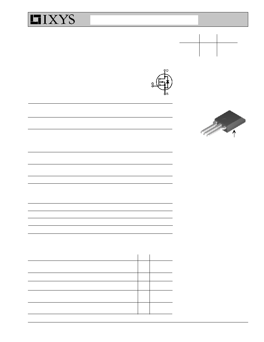
G = Gate,
D = Drain,
S = Source
* Patent pending
HiPerFET
TM
MOSFET
ISOPLUS220
TM
Electrically Isolated Back Surface
98851 (8/01)
G
D
S
ADVANCE TECHNICAL INFORMATION
ISOPLUS 220
TM
Features
l
Silicon chip on Direct-Copper-Bond
substrate
- High power dissipation
- Isolated mounting surface
- 2500V electrical isolation
l
Low drain to tab capacitance(<35pF)
l
Low R
DS (on)
l
Rugged polysilicon gate cell structure
l
Unclamped Inductive Switching (UIS)
rated
l
Fast intrinsic Rectifier
Applications
l
DC-DC converters
l
Battery chargers
l
Switched-mode and resonant-mode
power supplies
l
DC choppers
l
AC motor control
Advantages
l
Easy assembly: no screws or isolation
foils required
l
Space savings
l
High power density
l
Low collector capacitance to ground
(low EMI)
Isolated back surface*
IXFC 80N08
IXFC 80N085
V
DSS
I
D25
R
DS(on)
80 V
80 A 9 m
85 V
80 A 9 m
IXYS MOSFETS and IGBTs are covered by one or more of the following U.S. patents:
4,835,592
4,881,106
5,017,508
5,049,961
5,187,117
5,486,715
4,850,072
4,931,844
5,034,796
5,063,307
5,237,481
5,381,025
IXYS reserves the right to change limits, test conditions, and dimensions.
Symbol
Test Conditions
Characteristic Values
(T
J
= 25
∞
C, unless otherwise specified)
min.
typ.
max.
g
fs
V
DS
= 10 V; I
D
= I
T
Notes 1, 2
35
55
S
C
iss
4800
pF
C
oss
V
GS
= 0 V, V
DS
= 25 V, f = 1 MHz
1675
pF
C
rss
590
pF
t
d(on)
50
ns
t
r
V
GS
= 10 V, V
DS
= 0.5 V
DSS
,
75
ns
t
d(off)
I
D
= 0.5 I
D25
, R
G
= 2.5
(External)
95
ns
t
f
31
ns
Q
g(on)
180
nC
Q
gs
V
GS
= 10 V, V
DS
= 0.5 V
DSS
, I
D
= I
T
42
nC
Q
gd
Notes 2
75
nC
R
thJC
0.54
K/W
R
thCK
0.25
K/W
Source-Drain Diode
Characteristic Values
(T
J
= 25
∞
C, unless otherwise specified)
Symbol
Test Conditions
min.
typ.
max.
I
S
V
GS
= 0 V
80
A
I
SM
Repetitive; pulse width limited by T
JM
320
A
V
SD
I
F
= I
S
, V
GS
= 0 V,
1.5
V
Note 1
t
rr
200
ns
Q
RM
0.5
µ
C
I
RM
6
A
I
F
= 25A
-di/dt = 100 A/
µ
s,
V
R
= 50 V
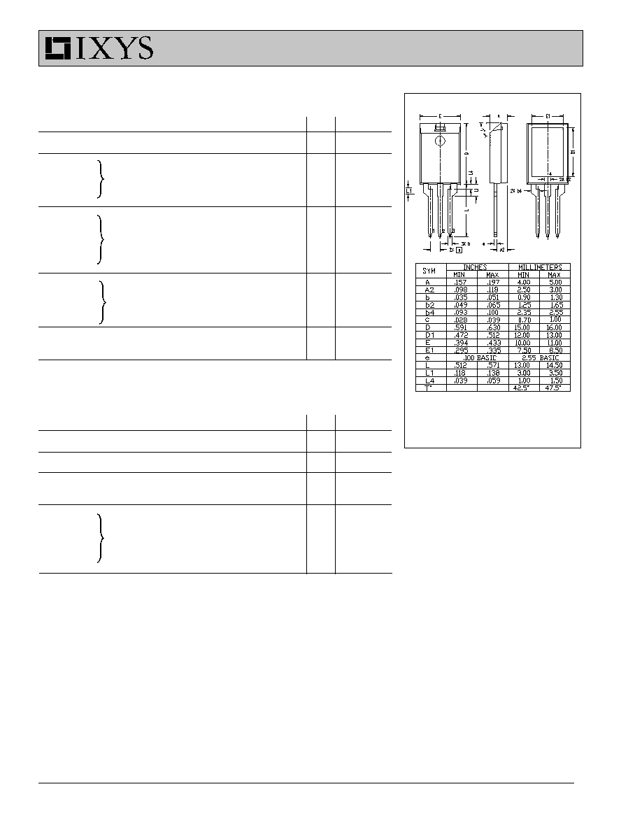
Note: All terminals are solder plated.
1 - Gate
2 - Drain
3 - Source
ISOPLUS220 OUTLINE
Note: 1. Pulse test, t
300
µ
s, duty cycle d
2 %
2. I
T
= 40A
IXFC 80N08
IXFC 80N085