
1 - 4
© 2000 IXYS All rights reserved
HiPerFET
TM
Power MOSFETs
N-Channel Enhancement Mode
High dv/dt, Low t
rr
, HDMOS
TM
Family
Symbol
Test Conditions
Maximum Ratings
V
DSS
T
J
= 25
∞
C to 150
∞
C
800
V
V
DGR
T
J
= 25
∞
C to 150
∞
C; R
GS
= 1 M
W
800
V
V
GS
Continuous
±
20
V
V
GSM
Transient
±
30
V
I
D25
T
C
= 25
∞
C
14N80
14
A
15N80
15
A
I
DM
T
C
= 25
∞
C, pulse width limited by T
JM
14N80
56
A
15N80
60
A
I
AR
T
C
= 25
∞
C
14N80
14
A
15N80
15
A
E
AR
T
C
= 25
∞
C
30
mJ
dv/dt
I
S
£
I
DM
, di/dt
£
100 A/
m
s, V
DD
£
V
DSS
,
5
V/ns
T
J
£
150
∞
C, R
G
= 2
W
P
D
T
C
= 25
∞
C
300
W
T
J
-55 ... +150
∞
C
T
JM
150
∞
C
T
stg
-55 ... +150
∞
C
T
L
1.6 mm (0.062 in.) from case for 10 s
300
∞
C
M
d
Mounting torque
1.13/10 Nm/lb.in.
Weight
6
g
Features
∑
International standard packages
∑
Low R
DS (on)
HDMOS
TM
process
∑
Rugged polysilicon gate cell structure
∑
Unclamped Inductive Switching (UIS)
rated
∑
Low package inductance
- easy to drive and to protect
∑
Fast intrinsic Rectifier
Applications
∑
DC-DC converters
∑
Synchronous rectification
∑
Battery chargers
∑
Switched-mode and resonant-mode
power supplies
∑
DC choppers
∑
AC motor control
∑
Temperature and lighting controls
∑
Low voltage relays
Advantages
∑
Easy to mount with 1 screw
(isolated mounting screw hole)
∑
Space savings
∑
High power density
TO-247 AD
Preliminary data
G = Gate
D = Drain
S = Source
TAB = Drain
(TAB)
96523B (3/98)
Symbol
Test Conditions
Characteristic Values
(T
J
= 25
∞
C, unless otherwise specified)
Min. Typ.
Max.
V
DSS
V
GS
= 0 V, I
D
= 3 mA
800
V
V
DSS
temperature coefficient
0.096
%/K
V
GS(th)
V
DS
= V
GS
, I
D
= 4 mA
2.0
4.5
V
V
GS(th)
temperature coefficient
-0.214
%/K
I
GSS
V
GS
=
±
20 V
DC
, V
DS
= 0
±
100
nA
I
DSS
V
DS
= 0.8 V
DSS
T
J
= 25
∞
C
250
m
A
V
GS
= 0 V
T
J
= 125
∞
C
1
mA
R
DS(on)
V
GS
= 10 V, I
D
= 0.5 I
D25
14N80
0.70
W
15N80
0.60
W
Pulse test, t
£
300
m
s, duty cycle d
£
2 %
V
DSS
I
D25
R
DS(on)
800 V
14 A
0.70
W
800 V
15 A
0.60
W
t
rr
£
250 ns
IXFH14N80
IXFH15N80
IXYS reserves the right to change limits, test conditions, and dimensions.

2 - 4
© 2000 IXYS All rights reserved
IXFH 14N80
IXFH 15N80
Symbol
Test Conditions
Characteristic Values
(T
J
= 25
∞
C, unless otherwise specified)
Min.
Typ.
Max.
g
fs
V
DS
= 10 V; I
D
= 0.5 I
D25
, pulse test
8
14
S
C
iss
3965
4870
pF
C
oss
V
GS
= 0 V, V
DS
= 25 V, f = 1 MHz
315
395
pF
C
rss
73
120
pF
t
d(on)
20
50
ns
t
r
V
GS
= 10 V, V
DS
= 0.5 V
DSS
, I
D
= 0.5 I
D25
33
50
ns
t
d(off)
R
G
= 2
W
(External)
63
100
ns
t
f
32
50
ns
Q
g(on)
128
155
nC
Q
gs
V
GS
= 10 V, V
DS
= 0.5 V
DSS
, I
D
= 0.5 I
D25
30
45
nC
Q
gd
55
80
nC
R
thJC
0.42
K/W
R
thCK
0.25
K/W
Source-Drain Diode
Characteristic Values
(T
J
= 25
∞
C, unless otherwise specified)
Symbol
Test Conditions
min.
typ.
max.
I
S
V
GS
= 0 V
14N80
14
A
15N80
15
A
I
SM
Repetitive;
14N80
56
A
15N80
60
A
V
SD
I
F
= I
S
, V
GS
= 0 V,
1.5
V
Pulse test, t
£
300
m
s, duty cycle d
£
2 %
t
rr
T
J
= 25
∞
C
250
ns
T
J
= 125
∞
C
400
ns
Q
RM
1
m
C
I
RM
8.5
A
I
F
= I
S
-di/dt = 100 A/
m
s,
V
R
= 100 V
TO-247 AD Outline
Dim. Millimeter
Inches
Min.
Max.
Min.
Max.
A
19.81 20.32
0.780 0.800
B
20.80 21.46
0.819 0.845
C
15.75 16.26
0.610 0.640
D
3.55
3.65
0.140 0.144
E
4.32
5.49
0.170 0.216
F
5.4
6.2
0.212 0.244
G
1.65
2.13
0.065 0.084
H
-
4.5
-
0.177
J
1.0
1.4
0.040 0.055
K
10.8
11.0
0.426 0.433
L
4.7
5.3
0.185 0.209
M
0.4
0.8
0.016 0.031
N
1.5
2.49
0.087 0.102
IXYS MOSFETS and IGBTs are covered by one or more of the following U.S. patents:
4,835,592
4,881,106
5,017,508
5,049,961
5,187,117
5,486,715
4,850,072
4,931,844
5,034,796
5,063,307
5,237,481
5,381,025

3 - 4
© 2000 IXYS All rights reserved
V
GS
- Volts
2
3
4
5
6
7
I
D
- A
m
pere
s
0
2
4
6
8
10
12
14
16
T
C
- Degrees C
-50 -25
0
25
50
75
100 125 150
I
D
- A
m
pere
s
0
4
8
12
16
20
T
J
- Degrees C
25
50
75
100
125
150
R
DS
(
O
N)
-
N
o
r
m
alized
1.0
1.2
1.4
1.6
1.8
2.0
2.2
2.4
2.6
I
D
= 7.5A
I
D
- Amperes
0
5
10
15
20
25
R
DS
(
O
N)
- N
o
rm
ali
z
ed
0.8
1.0
1.2
1.4
1.6
1.8
2.0
2.2
2.4
2.6
V
DS
- Volts
0
4
8
12
16
20
I
D
- A
m
pe
res
0
4
8
12
16
20
V
DS
- Volts
0
2
4
6
8
10
I
D
- A
m
p
e
r
e
s
0
4
8
12
16
20
4V
V
GS
= 10V
V
GS
= 9V
8V
7V
6V
T
J
= 125
O
C
V
GS
= 10V
T
J
= 25
O
C
5V
5V
4V
T
J
= 25
o
C
I
D
= 15A
T
J
= 25
O
C
IXFH14N80
IXFH15N80
T
J
= 125
o
C
V
GS
= 9V
8V
7V
6V
T
J
= 125
O
C
IXFH 14N80
IXFH 15N80
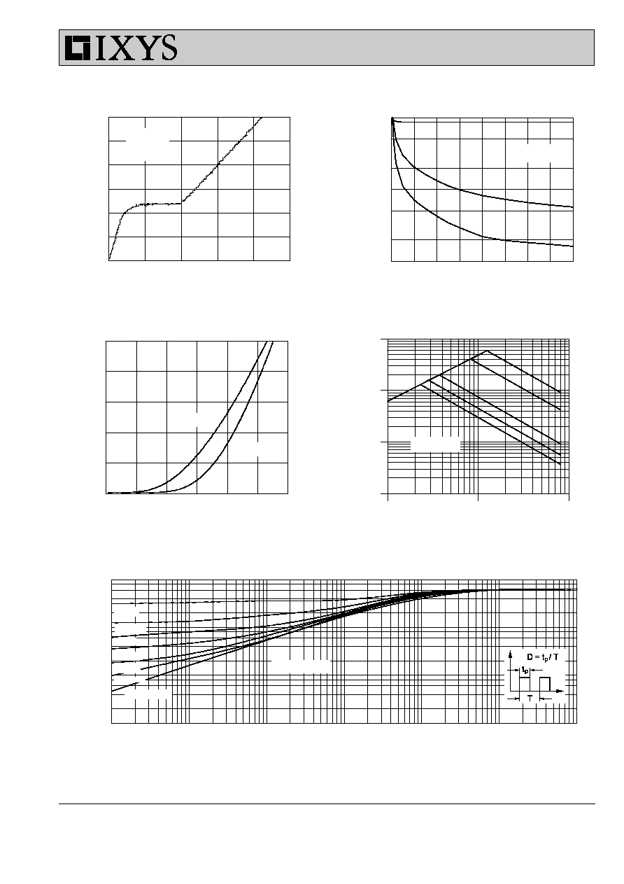
Figure 3. R
DS(on)
normalized to 0.5 I
D25
value vs. I
D
Figure 5. Drain Current vs. Case Temperature
Figure 6. Admittance Curves
Figure 1. Output Characteristics at 25
O
C
Figure 2. Output Characteristics at 125
O
C
Figure 4. R
DS(on)
normalized to 0.5 I
D25
value vs. T
J
4 - 4
© 2000 IXYS All rights reserved
IXFH 14N80
IXFH 15N80
V
DS
- Volts
1 0
1 00
1 000
I
D
-
A
m
p
e
res
0. 1
1
1 0
1 00
Pulse Width - Seconds
0.00001
0.0001
0.001
0.01
0.1
1
10
R(th)
JC
- K/W
0.001
0.01
0.1
1
V
DS
- Volts
0
5
10
15
20
25
30
35
40
Cap
a
c
i
ta
nc
e -
p
F
50
100
250
500
1000
2500
5000
V
SD
- Volts
0.2
0.4
0.6
0.8
1.0
1.2
1.4
I
D
-
A
m
pe
r
e
s
0
10
20
30
40
50
Gate Charge - nC
0
50
100
150
200
250
V
GS
-
V
o
lt
s
0
2
4
6
8
10
12
Crss
Coss
Ciss
V
DS
= 400V
I
D
= 15A
I
G
= 1mA
f = 1MHz
T
C
= 25
O
C
10ms
1ms
100ms
DC
T
J
= 125
O
C
Single pulse
D = Duty Cycle
0.1ms
T
J
= 25
O
C
D=0.5
D=0.1
D=0.05
D=0.02
D=0.01
D=0.2
Figure 8. Capacitance Curves
Figure 7. Gate Charge
Figure 9. Source Current vs. Source to Drain Voltage
Figure 11. Transient Thermal Resistance
Figure10. Forward Bias Safe Operating Area