© 2003 IXYS All rights reserved
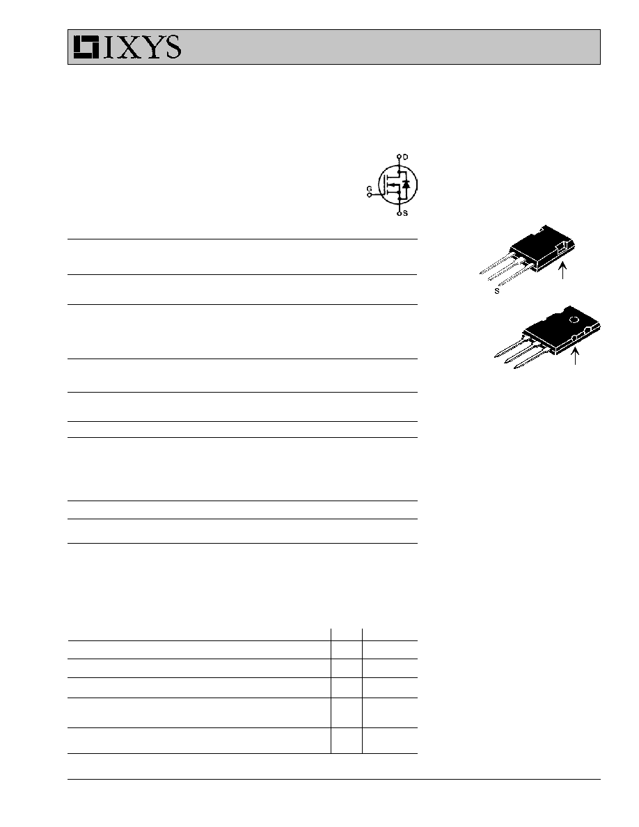
Symbol
Test Conditions
Maximum Ratings
V
DSS
T
J
= 25
∞
C to 150
∞
C
70
V
V
DGR
T
J
= 25
∞
C to 150
∞
C; R
GS
= 1 M
70
V
V
GS
Continuous
±
20
V
V
GSM
Transient
±
30
V
I
D25
T
C
= 25
∞
C (MOSFET chip capability)
180
A
I
D(RMS)
External lead (current limit)
76
A
I
DM
T
C
= 25
∞
C, Note 1
720
A
I
AR
T
C
= 25
∞
C
180
A
E
AR
T
C
= 25
∞
C
60
mJ
E
AS
T
C
= 25
∞
C
3
J
dv/dt
I
S
I
DM
, di/dt
100 A/
µ
s, V
DD
V
DSS
5
V/ns
T
J
150
∞
C, R
G
= 2
P
D
T
C
= 25
∞
C
560
W
T
J
-55 ... +150
∞
C
T
JM
150
∞
C
T
stg
-55 ... +150
∞
C
T
L
1.6 mm (0.063 in.) from case for 10 s
300
∞
C
M
d
Mounting torque
TO-264
0.9/6
Nm/lb.in.
Weight
PLUS 247
6 g
TO-264
10 g
Symbol
Test Conditions
Characteristic Values
(T
J
= 25
∞
C, unless otherwise specified)
min.
typ.
max.
V
DSS
V
GS
= 0 V, I
D
= 3mA
70
V
V
GS(th)
V
DS
= V
GS
, I
D
= 8mA
2.0
4.0 V
I
GSS
V
GS
=
±
20 V, V
DS
= 0
±
100 nA
I
DSS
V
DS
= V
DSS
T
J
= 25
∞
C
100
µ
A
V
GS
= 0 V
T
J
= 125
∞
C
2 mA
R
DS(on)
V
GS
= 10 V, I
D
= 0.5 ∑ I
D25
6 m
Note 2
Single MOSFET Die
Features
International standard packages
Low R
DS (on)
HDMOS
TM
process
Rugged polysilicon gate cell structure
Unclamped Inductive Switching (UIS)
rated
Low package inductance
- easy to drive and to protect
Fast intrinsic rectifier
Applications
DC-DC converters
Synchronous rectification
Battery chargers
Switched-mode and resonant-mode
power supplies
DC choppers
Temperature and lighting controls
Low voltage relays
Advantages
PLUS 247
TM
package for clip or spring
mounting
Space savings
High power density
HiPerFET
TM
Power MOSFETs
DS98556C(01/03)
PLUS 247
TM
G
D
D (TAB)
G = Gate
D = Drain
S = Source
TAB = Drain
IXFK 180N07
V
DSS
= 70
V
IXFX 180N07
I
D25
= 180
A
R
DS(on)
=
6
m
t
rr
250 ns
S
G
D
(TAB)
TO-264 AA (IXFK)
Preliminary Data Sheet
IXYS reserves the right to change limits, test conditions, and dimensions.
IXYS MOSFETS and IGBTs are covered by one or more of the following U.S. patents:
4,835,592
4,881,106
5,017,508
5,049,961
5,187,117
5,486,715
6,306,728B1
4,850,072
4,931,844
5,034,796
5,063,307
5,237,481
5,381,025
Symbol
Test Conditions
Characteristic Values
(T
J
= 25
∞
C, unless otherwise specified)
min.
typ.
max.
g
fs
V
DS
= 10 V; I
D
= 60A
Note 2
55
90
S
C
iss
9400
pF
C
oss
V
GS
= 0 V, V
DS
= 25 V, f = 1 MHz
4600
pF
C
rss
2550
pF
t
d(on)
65
ns
t
r
V
GS
= 10 V, V
DS
= 0.5 ∑ V
DSS
, I
D
= 0.5 ∑ I
D25
90
ns
t
d(off)
R
G
= 1
(External),
140
ns
t
f
55
ns
Q
g(on)
420
nC
Q
gs
V
GS
= 10 V, V
DS
= 0.5 ∑ V
DSS
, I
D
= 0.5 ∑ I
D25
65
nC
Q
gd
220
nC
R
thJC
0.22
K/W
R
thCK
0.15
K/W
Source-Drain Diode
Characteristic Values
(T
J
= 25
∞
C, unless otherwise specified)
Symbol
Test Conditions
min.
typ.
max.
I
S
V
GS
= 0 V
180
A
I
SM
Repetitive;
720
A
pulse width limited by T
JM
V
SD
I
F
= 100A, V
GS
= 0 V, Note 1
1.3
V
t
rr
250
ns
Q
RM
1.2
µ
C
I
RM
10
A
I
F
= 50A,-di/dt = 100 A/
µ
s, V
R
= 50 V
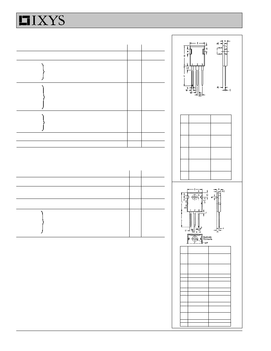
Dim.
Millimeter
Inches
Min.
Max.
Min. Max.
A
4.83
5.21
.190
.205
A
1
2.29
2.54
.090
.100
A
2
1.91
2.16
.075
.085
b
1.14
1.40
.045
.055
b
1
1.91
2.13
.075
.084
b
2
2.92
3.12
.115
.123
C
0.61
0.80
.024
.031
D
20.80
21.34
.819
.840
E
15.75
16.13
.620
.635
e
5.45 BSC
.215 BSC
L
19.81
20.32
.780
.800
L1
3.81
4.32
.150
.170
Q
5.59
6.20
.220 0.244
R
4.32
4.83
.170
.190
Terminals:
1 - Gate
2 - Drain (Collector)
3 - Source (Emitter)
4 - Drain (Collector)
PLUS 247
TM
Outline
Note: 1. Pulse width limited by T
JM
2. Pulse test, t
300
µ
s, duty cycle d
2 %
IXFK 180N07
IXFX 180N07
TO-264 AA Outline
Millimeter
Inches
Min.
Max.
Min.
Max.
A
4.82
5.13
.190
.202
A1
2.54
2.89
.100
.114
A2
2.00
2.10
.079
.083
b
1.12
1.42
.044
.056
b1
2.39
2.69
.094
.106
b2
2.90
3.09
.114
.122
c
0.53
0.83
.021
.033
D
25.91
26.16
1.020
1.030
E
19.81
19.96
.780
.786
e
5.46 BSC
.215 BSC
J
0.00
0.25
.000
.010
K
0.00
0.25
.000
.010
L
20.32
20.83
.800
.820
L1
2.29
2.59
.090
.102
P
3.17
3.66
.125
.144
Q
6.07
6.27
.239
.247
Q1
8.38
8.69
.330
.342
R
3.81
4.32
.150
.170
R1
1.78
2.29
.070
.090
S
6.04
6.30
.238
.248
T
1.57
1.83
.062
.072
Dim.