© 2000 IXYS All rights reserved
Features
International standard packages
miniBLOC,
with Aluminium nitride
isolation
Low R
DS (on)
HDMOS
TM
process
Rugged polysilicon gate cell structure
Unclamped Inductive Switching (UIS)
rated
Low package inductance
Fast intrinsic Rectifier
Applications
DC-DC converters
Battery chargers
Switched-mode and resonant-mode
power supplies
DC choppers
Temperature and lighting controls
Advantages
Easy to mount
Space savings
High power density
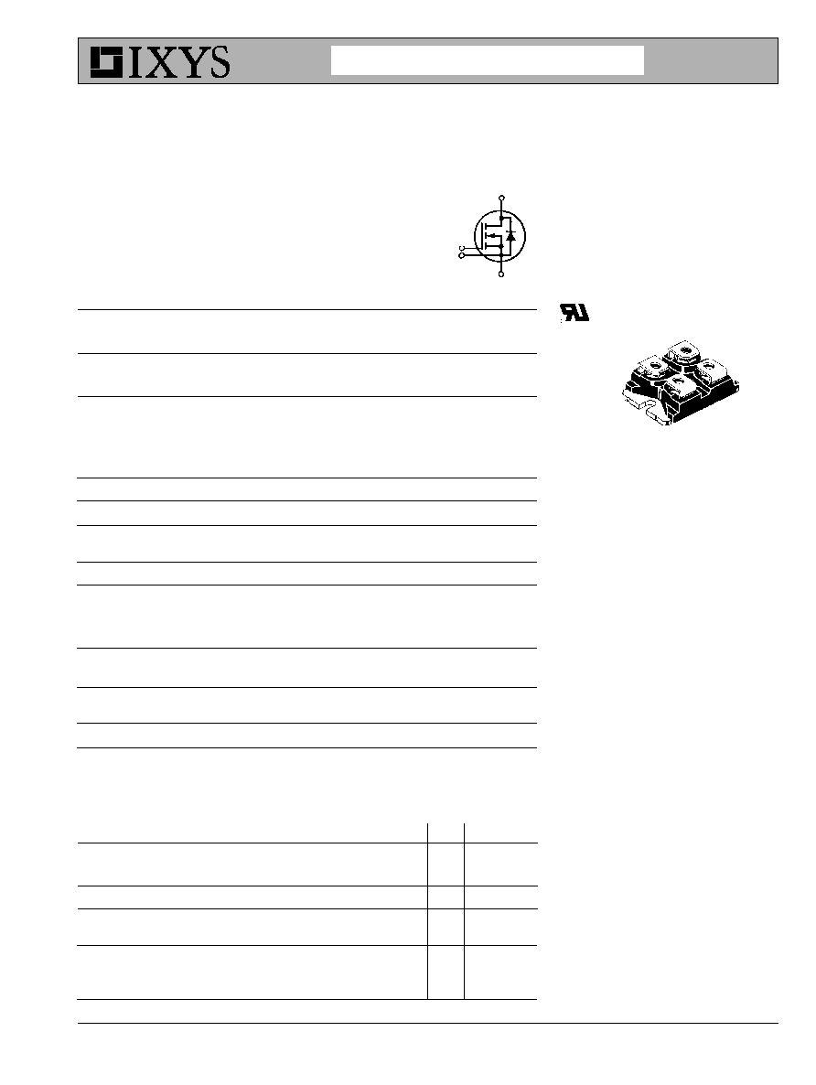
Symbol
Test Conditions
Characteristic Values
(T
J
= 25
∞
C, unless otherwise specified)
min.
typ.
max.
V
DSS
V
GS
= 0 V, I
D
= 3 mA
60
V
V
GH(th)
V
DS
= V
GS
, I
D
= 8 mA
2.0
4.0
V
I
GSS
V
GS
=
±
20 V
DC
, V
DS
= 0
±
200
nA
I
DSS
V
DS
= V
DSS
T
J
= 25
∞
C
100
m
A
V
GS
= 0 V
T
J
= 125
∞
C
2
mA
R
DS(on)
V
GS
= 10 V, I
D
= 100A
3
m
W
Pulse test, t
£
300
m
s,
duty cycle d
£
2 %
Symbol
Test Conditions
Maximum Ratings
V
DSS
T
J
= 25
∞
C to 150
∞
C
60
V
V
DGR
T
J
= 25
∞
C to 150
∞
C; R
GS
= 1 M
W
60
V
V
GS
Continuous
±
20
V
V
GSM
Transient
±
30
V
I
D25
T
C
= 25
∞
C, Chip capability
340
A
I
L(RMS)
Terminal current limit
100
A
I
DM
T
C
= 25
∞
C, pulse width limited by T
JM
1360
A
I
AR
T
C
= 25
∞
C
200
A
E
AR
T
C
= 25
∞
C
64
mJ
E
AS
T
C
= 25
∞
C
4
J
dv/dt
I
S
£
I
DM
, di/dt
£
100 A/
m
s, V
DD
£
V
DSS
,
5
V/ns
T
J
£
150
∞
C, R
G
= 2
W
P
D
T
C
= 25
∞
C
700
W
T
J
-55 ... +150
∞
C
T
JM
150
∞
C
T
stg
-55 ... +150
∞
C
V
ISOL
50/60 Hz, RMS
t = 1 min
2500
V~
I
ISOL
£
1 mA
t = 1 s
3000
V~
M
d
Mounting torque
1.5/13 Nm/lb.in.
Terminal connection torque
1.5/13 Nm/lb.in.
Weight
30
g
HiPerFET
TM
Power MOSFETs
Single Die MOSFET
N-Channel Enhancement Mode
Avalanche Rated, High dv/dt, Low t
rr
98751 (10/00)
D
S
G
S
S
G
S
D
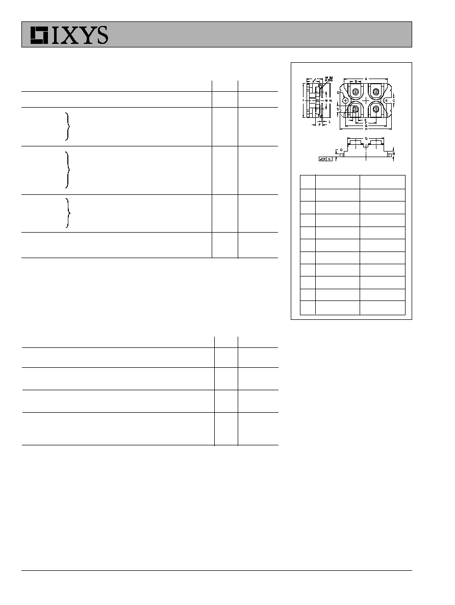
miniBLOC, SOT-227 B (IXFN)
E153432
G = Gate
D = Drain
S = Source
Either Source terminal at miniBLOC can be used
as Main or Kelvin Source
Advanced Technical Information
IXFN 340N06
V
DSS
= 60 V
I
D25
= 340 A
R
DS(on)
= 3
m
W
t
rr
£
250 ns
IXYS MOSFETS and IGBTs are covered by one or more of the following U.S. patents:
4,835,592
4,881,106
5,017,508
5,049,961
5,187,117
5,486,715
4,850,072
4,931,844
5,034,796
5,063,307
5,237,481
5,381,025
IXYS reserves the right to change limits, test conditions, and dimensions.
IXFN 340N06
Symbol
Test Conditions
Characteristic Values
(T
J
= 25∞C, unless otherwise specified)
min.
typ. max.
g
fs
V
DS
= 10 V; I
D
= 60A, pulse test
80
105
S
C
iss
16800
pF
C
oss
V
GS
= 0 V, V
DS
= 25 V, f = 1 MHz
8200
pF
C
rss
5000
pF
t
d(on)
140
ns
t
r
V
GS
= 10 V, V
DS
= 0.5 V
DSS
, I
D
= 100A
95
ns
t
d(off)
R
G
= 2 W (External),
200
ns
t
f
33
ns
Q
g(on)
600
nC
Q
gs
V
GS
= 10 V, V
DS
= 50V, I
D
= 100A
110
nC
Q
gd
300
nC
R
thJC
0.18 K/W
R
thCK
0.05
K/W
Source-Drain Diode
Characteristic Values
(T
J
= 25∞C, unless otherwise specified)
Symbol
Test Conditions
min.
typ. max.
I
S
V
GS
= 0 V
340
A
I
SM
Repetitive;1360
A
pulse width limited by T
JM
V
SD
I
F
= 100A, V
GS
= 0 V,
1.2
V
Pulse test, t £ 300 ms, duty cycle d £ 2 %
t
rr
I
F
= 50A, -di/dt = 100 A/ms, V
R
= 40V; T
J
=25∞C
250
ns
Q
RM
1.4
mC
I
RM
8
A
miniBLOC, SOT-227 B
M4 screws (4x) supplied
Dim.
Millimeter
Inches
Min.
Max.
Min.
Max.
A
31.50
31.88
1.240
1.255
B
7.80
8.20
0.307
0.323
C
4.09
4.29
0.161
0.169
D
4.09
4.29
0.161
0.169
E
4.09
4.29
0.161
0.169
F
14.91
15.11
0.587
0.595
G
30.12
30.30
1.186
1.193
H
38.00
38.23
1.496
1.505
J
11.68
12.22
0.460
0.481
K
8.92
9.60
0.351
0.378
L
0.76
0.84
0.030
0.033
M
12.60
12.85
0.496
0.506
N
25.15
25.42
0.990
1.001
O
1.98
2.13
0.078
0.084
P
4.95
5.97
0.195
0.235
Q
26.54
26.90
1.045
1.059
R
3.94
4.42
0.155
0.174
S
4.72
4.85
0.186
0.191
T
24.59
25.07
0.968
0.987
U
-0.05
0.1
-0.002
0.004