DATASHEET SEARCH SITE | WWW.ALLDATASHEET.COM
© 2004 IXYS All rights reserved
Symbol
Test Conditions
Maximum Ratings
V
DSS
T
J
= 25
°C to 150°C
1000
V
V
DGR
T
J
= 25
°C to 150°C; R
GS
= 1 M
1000
V
V
GS
Continuous
±20
V
V
GSM
Transient
±30
V
I
D25
T
C
= 25
°C
10N100
10
A
12N100
12
A
I
DM
T
C
= 25
°C, pulse width limited by T
JM
10N100
40
A
12N100
48
A
I
AR
T
C
= 25
°C
10N100
10
A
12N100
12
A
E
AR
T
C
= 25
°C
30
mJ
dv/dt
I
S
I
DM
, di/dt
100 A/µs, V
DD
V
DSS
,
5
V/ns
T
J
150°C, R
G
= 2
P
D
T
C
= 25
°C
300
W
T
J
-55 ... +150
°C
T
JM
150
°C
T
stg
-55 ... +150
°C
T
L
1.6 mm (0.062 in.) from case for 10 s
300
°C
M
d
Mounting torque
1.13/10 Nm/lb.in.
Weight
TO-268 = 6 g
Symbol
Test Conditions
Characteristic Values
(T
J
= 25
°C, unless otherwise specified)
min.
typ.
max.
V
DSS
V
GS
= 0 V, I
D
= 3 mA
1000
V
V
GS(th)
V
DS
= V
GS
, I
D
= 4 mA
2.0
4.5
V
I
GSS
V
GS
=
±20 V
DC
, V
DS
= 0
±100
nA
I
DSS
V
DS
= 0.8 · V
DSS
T
J
= 25
°C
250
µA
V
GS
= 0 V
T
J
= 125
°C
1 mA
R
DS(on)
V
GS
= 10 V, I
D
= 0.5 · I
D25
10N100
1.20
12N100
1.05
Pulse test, t
300 µs, duty cycle d 2 %
G = Gate,
TAB = Drain
S = Source,
Features
International standard package
Low R
DS (on)
HDMOS
TM
process
Rugged polysilicon gate cell
structure
Unclamped Inductive Switching (UIS)
rated
Low package inductance
- easy to drive and to protect
Fast intrinsic Rectifier
Applications
DC-DC converters
Synchronous rectification
Battery chargers
Switched-mode and resonant-mode
power supplies
DC choppers
AC motor control
Temperature and lighting controls
Low voltage relays
Advantages
Surface mountable, high power
package
Space savings
High power density
V
DSS
I
D25
R
DS(on)
IXFT
10
N100 1000 V 10 A 1.20
IXFT12
N100 1000 V 12 A 1.05
t
rr
250 ns
HiPerFET
TM
Power MOSFETs
N-Channel Enhancement Mode
High dv/dt, Low t
rr
, HDMOS
TM
Family
DS98509A(01/04)
Preliminary data sheet
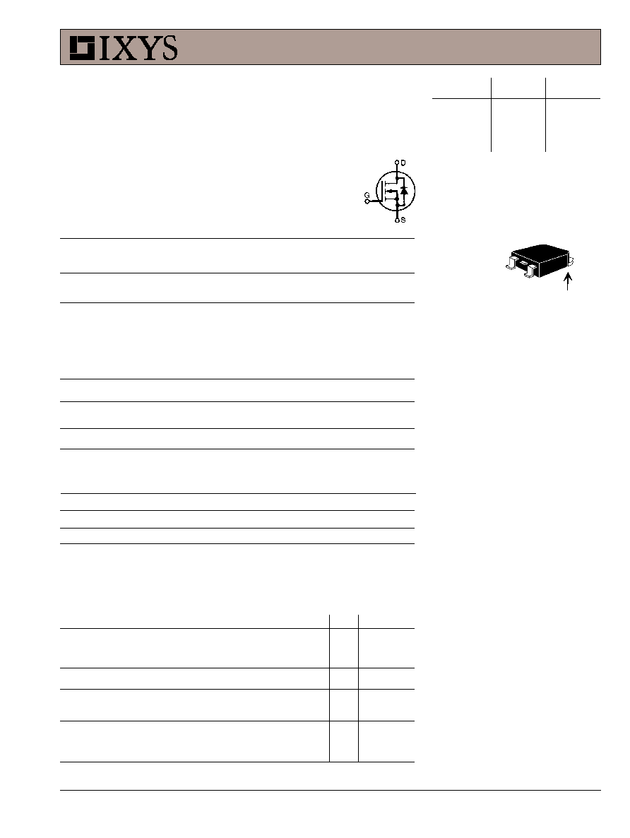
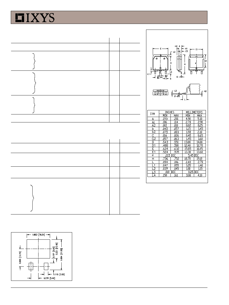
TO-268 Case Style
(TAB)
G
S
IXYS reserves the right to change limits, test conditions, and dimensions.
IXYS MOSFETs and IGBTs are covered by one or more
of the following U.S. patents:
4,835,592 4,881,106 5,017,508 5,049,961 5,187,117 5,486,715 6,306,728B1 6,259,123B1 6,306,728B1
4,850,072 4,931,844 5,034,796 5,063,307 5,237,481 5,381,025 6,404,065B1 6,162,665 6,534,343 6,583,505
Symbol
Test Conditions
Characteristic Values
(T
J
= 25
°C, unless otherwise specified)
min.
typ.
max.
g
fs
V
DS
= 10 V; I
D
= 0.5 · I
D25
, pulse test
6
10
S
C
iss
4000
pF
C
oss
V
GS
= 0 V, V
DS
= 25 V, f = 1 MHz
310
pF
C
rss
70
pF
t
d(on)
21
50
ns
t
r
V
GS
= 10 V, V
DS
= 0.5 · V
DSS
, I
D
= 0.5 · I
D25
33
50
ns
t
d(off)
R
G
= 2
(External),
62 100
ns
t
f
32
50
ns
Q
g(on)
122 155
nC
Q
gs
V
GS
= 10 V, V
DS
= 0.5 · V
DSS
, I
D
= 0.5 · I
D25
30
45
nC
Q
gd
50
80
nC
R
thJC
0.42
K/W
Source-Drain Diode
Characteristic Values
(T
J
= 25
°C, unless otherwise specified)
Symbol
Test Conditions
min.
typ.
max.
I
S
V
GS
= 0 V
10N100
10
A
12N100
12
A
I
SM
Repetitive;
10N100
40
A
pulse width limited by T
JM
12N100
48
A
V
SD
I
F
= I
S
, V
GS
= 0 V,
1.5
V
Pulse test, t
300 µs, duty cycle d 2 %
t
rr
T
J
= 25
°C
250
ns
T
J
= 125
°C
400
ns
Q
RM
T
J
= 25
°C
1
µC
T
J
= 125
°C
2
µC
I
RM
T
J
= 25
°C
10
A
T
J
= 125
°C
15
A
I
F
= I
S
-di/dt = 100 A/
µs,
V
R
= 100 V
TO-268 Outline
Min Recommended Footprint
IXFT 10N100 IXFT 12N100
© 2004 IXYS All rights reserved
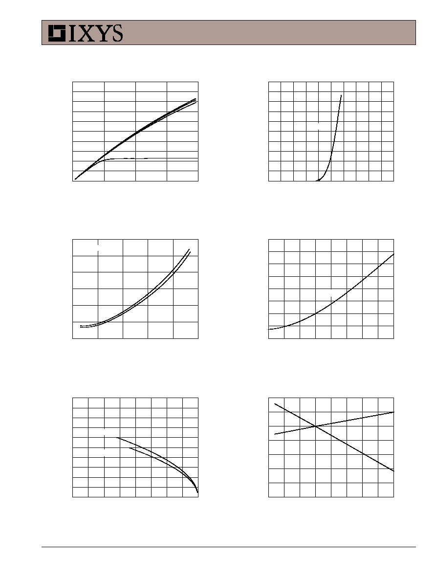
Fig. 1. Output Characteristics
Fig. 2. Input Admittance
Fig. 5. Drain vs. Case Temperature
Fig. 6. Temperature Dependence of
Breakdown and Threshold Voltage
Fig. 3. R
DS(on)
vs. Drain Current
Fig. 4. Temperature Dependence
of Drain to Source Resistance
T
J
- Degrees C
-50 -25
0
25
50
75
100 125 150
BV/
V
G(
t
h
)
- N
o
rm
a
l
i
z
e
d
0.5
0.6
0.7
0.8
0.9
1.0
1.1
1.2
BV
DSS
V
GS(th)
T
C
- Degrees C
-50 -25
0
25
50
75
100 125 150
I
D
-
A
m
per
es
0
2
4
6
8
10
12
14
16
18
20
10N100
T
J
- Degrees C
-50 -25
0
25
50
75
100 125 150
R
DS
(
on)
- No
rm
a
l
i
z
e
d
0.50
0.75
1.00
1.25
1.50
1.75
2.00
2.25
2.50
I
D
- Amperes
0
5
10
15
20
25
R
DS
(
on)
- No
rm
a
l
i
z
e
d
0.9
1.0
1.1
1.2
1.3
1.4
1.5
V
GS
= 10V
V
GS
- Volts
0
1
2
3
4
5
6
7
8
9
10
I
D
-
Am
per
es
0
2
4
6
8
10
12
14
16
18
20
V
DS
- Volts
0
5
10
15
20
I
D
-
Am
per
es
0
2
4
6
8
10
12
14
16
18
20
6V
7V
V
GS
= 10V
12N100
I
D
= 6A
V
GS
= 15V
5V
T
J
= 25°C
T
J
= 25°C
T
J
= 25°C
IXFT 10N100 IXFT 12N100
IXYS reserves the right to change limits, test conditions, and dimensions.
IXYS MOSFETs and IGBTs are covered by one or more
of the following U.S. patents:
4,835,592 4,881,106 5,017,508 5,049,961 5,187,117 5,486,715 6,306,728B1 6,259,123B1 6,306,728B1
4,850,072 4,931,844 5,034,796 5,063,307 5,237,481 5,381,025 6,404,065B1 6,162,665 6,534,343 6,583,505
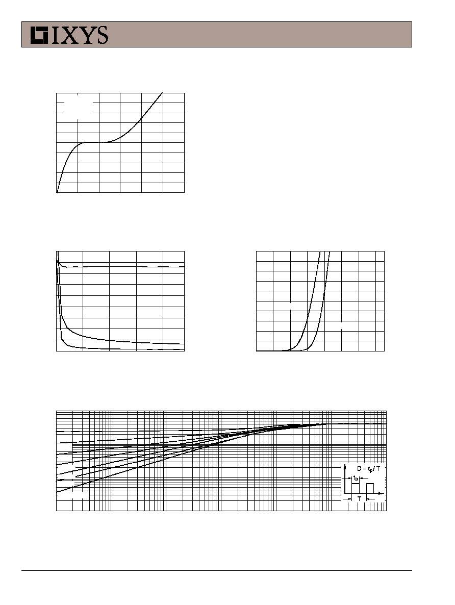
Fig. 7. Gate Charge Characteristic Curve
Fig. 8. Capacitance Curves
Fig. 9. Source Current vs. Source
to Drain Voltage
Fig.10.
Transient Thermal Impedance
V
DS
- Volts
1
10
100
1000
I
D
-
A
m
peres
0.1
1
10
Gate Charge - nCoulombs
0
25
50
75
100
125
150
V
GS
-
V
o
lt
s
0
1
2
3
4
5
6
7
8
9
10
V
SD
- Volts
0.0
0.2
0.4
0.6
0.8
1.0
1.2
1.4
I
D
- A
m
p
e
r
e
s
0
2
4
6
8
10
12
14
16
18
20
V
DS
- Volts
0
5
10
15
20
Ca
pacit
a
n
ce
-
pF
0
500
1000
1500
2000
2500
3000
3500
4000
4500
Time - Seconds
0.00001
0.0001
0.001
0.01
0.1
1
10
T
herm
a
l
R
e
sp
onse
-
K
/
W
0.001
0.01
0.1
1
D=0.5
C
rss
C
oss
10µs
100µs
1ms
10ms
100ms
C
iss
Limited by R
DS(on)
V
DS
= 500V
I
D
= 6A
I
G
= 10mA
Single Pulse
f = 1MHz
V
DS
= 25V
T
J
= 125°C
T
J
= 25°C
D=0.2
D=0.1
D=0.05
D=0.01
D=0.02
IXFT 10N100 IXFT 12N100