1 - 4
© 2000 IXYS All rights reserved
Symbol
Test Conditions
Maximum Ratings
V
DSS
T
J
= 25
∞
C to 150
∞
C
100
V
V
DGR
T
J
= 25
∞
C to 150
∞
C; R
GS
= 1 M
W
100
V
V
GS
Continuous
±
20
V
V
GSM
Transient
±
30
V
I
D25
T
C
= 25
∞
C (MOSFET chip capability)
180
A
I
D(RMS)
External lead (current limit)
76
A
I
DM
T
C
= 25
∞
C, Note 1
720
A
I
AR
T
C
= 25
∞
C
180
A
E
AR
T
C
= 25
∞
C
60
mJ
E
AS
T
C
= 25
∞
C
3
J
dv/dt
I
S
£
I
DM
, di/dt
£
100 A/
m
s, V
DD
£
V
DSS
5
V/ns
T
J
£
150
∞
C, R
G
= 2
W
P
D
T
C
= 25
∞
C
560
W
T
J
-55 ... +150
∞
C
T
JM
150
∞
C
T
stg
-55 ... +150
∞
C
T
L
1.6 mm (0.063 in.) from case for 10 s
300
∞
C
M
d
Mounting torque
TO-264
0.9/6
Nm/lb.in.
Weight
PLUS 247
6
g
TO-264
10 g
Symbol
Test Conditions
Characteristic Values
(T
J
= 25
∞
C, unless otherwise specified)
min.
typ.
max.
V
DSS
V
GS
= 0 V, I
D
= 3mA
100
V
V
GS(th)
V
DS
= V
GS
, I
D
= 8mA
2.0
4.0 V
I
GSS
V
GS
=
±
20 V, V
DS
= 0
±
100 nA
I
DSS
V
DS
= V
DSS
T
J
= 25
∞
C
100
m
A
V
GS
= 0 V
T
J
= 125
∞
C
2 mA
R
DS(on)
V
GS
= 10 V, I
D
= 0.5 ∑ I
D25
8 m
W
Note 1
Single MOSFET Die
Features
∑ International standard packages
∑ Low R
DS (on)
HDMOS
TM
process
∑ Rugged polysilicon gate cell structure
∑ Unclamped Inductive Switching (UIS)
rated
∑ Low package inductance
- easy to drive and to protect
∑ Fast intrinsic rectifier
Applications
∑ DC-DC converters
∑ Battery chargers
∑ Switched-mode and resonant-mode
power supplies
∑ DC choppers
∑ AC motor control
∑ Temperature and lighting controls
Advantages
∑ PLUS 247
TM
package for clip or spring
mounting
∑ Space savings
∑ High power density
HiPerFET
TM
Power MOSFETs
98552B (7/99)
PLUS 247
TM
(IXFX)
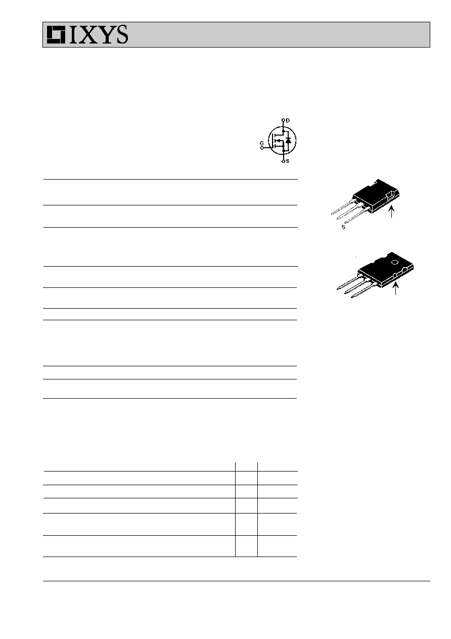
G
D
D (TAB)
G = Gate
D = Drain
S = Source
TAB = Drain
IXFK 180N10
V
DSS
= 100 V
IXFX 180N10
I
D25
= 180 A
R
DS(on)
=
8 m
W
t
rr
£
250 ns
S
G
D
(TAB)
TO-264 AA (IXFK)
Preliminary data sheet
IXYS reserves the right to change limits, test conditions, and dimensions.
2 - 4
© 2000 IXYS All rights reserved
Symbol
Test Conditions
Characteristic Values
(T
J
= 25
∞
C, unless otherwise specified)
min.
typ.
max.
g
fs
V
DS
= 10 V; I
D
= 60A
Note 2
60
90
S
C
iss
9100
pF
C
oss
V
GS
= 0 V, V
DS
= 25 V, f = 1 MHz
3200
pF
C
rss
1660
pF
t
d(on)
50
ns
t
r
V
GS
= 10 V, V
DS
= 0.5 ∑ V
DSS
, I
D
= 0.5 ∑ I
D25
90
ns
t
d(off)
R
G
= 1
W
(External),
140
ns
t
f
65
ns
Q
g(on)
360
nC
Q
gs
V
GS
= 10 V, V
DS
= 0.5 ∑ V
DSS
, I
D
= 0.5 ∑ I
D25
65
nC
Q
gd
190
nC
R
thJC
0.22
K/W
R
thCK
0.15
K/W
Source-Drain Diode
Characteristic Values
(T
J
= 25
∞
C, unless otherwise specified)
Symbol
Test Conditions
min.
typ.
max.
I
S
V
GS
= 0 V
180
A
I
SM
Repetitive;
720
A
pulse width limited by T
JM
V
SD
I
F
= 100A, V
GS
= 0 V, Note 1
1.5
V
t
rr
250
ns
Q
RM
1.1
m
C
I
RM
13
A
I
F
= 50A,-di/dt = 100 A/
m
s, V
R
= 50 V
Note: 1. Pulse width limited by T
JM
2. Pulse test, t
£
300
m
s, duty cycle d
£
2 %
IXFK 180N10
IXFX 180N10
PLUS247
TM
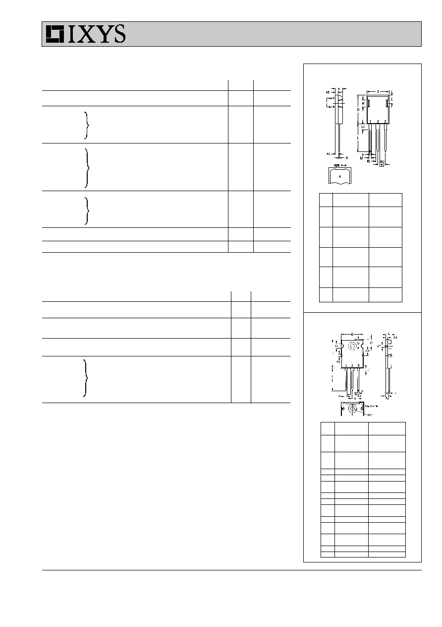
(IXFX) Outline
Dim.
Millimeter
Inches
Min.
Max.
Min. Max.
A
4.83
5.21
.190 .205
A
1
2.29
2.54
.090 .100
A
2
1.91
2.16
.075 .085
b
1.14
1.40
.045 .055
b
1
1.91
2.13
.075 .084
b
2
2.92
3.12
.115 .123
C
0.61
0.80
.024 .031
D
20.80
21.34
.819 .840
E
15.75
16.13
.620 .635
e 5.45 BSC
.215 BSC
L
19.81
20.32
.780 .800
L1
3.81
4.32
.150 .170
Q
5.59
6.20
.220 .244
R
4.32
4.83
.170 .190
Millimeter
Inches
Min.
Max.
Min.
Max.
A
4.82
5.13
.190
.202
A1
2.54
2.89
.100
.114
A2
2.00
2.10
.079
.083
b
1.12
1.42
.044
.056
b1
2.39
2.69
.094
.106
b2
2.90
3.09
.114
.122
c
0.53
0.83
.021
.033
D
25.91
26.16
1.020
1.030
E
19.81
19.96
.780
.786
e
5.46 BSC
.215 BSC
J
0.00
0.25
.000
.010
K
0.00
0.25
.000
.010
L
20.32
20.83
.800
.820
L1
2.29
2.59
.090
.102
P
3.17
3.66
.125
.144
Q
6.07
6.27
.239
.247
Q1
8.38
8.69
.330
.342
R
3.81
4.32
.150
.170
R1
1.78
2.29
.070
.090
S
6.04
6.30
.238
.248
T
1.57
1.83
.062
.072
Dim.
TO-264 AA (IXFK) Outline
IXYS MOSFETS and IGBTs are covered by one or more of the following U.S. patents:
4,835,592
4,881,106
5,017,508
5,049,961
5,187,117
5,486,715
4,850,072
4,931,844
5,034,796
5,063,307
5,237,481
5,381,025
3 - 4
© 2000 IXYS All rights reserved
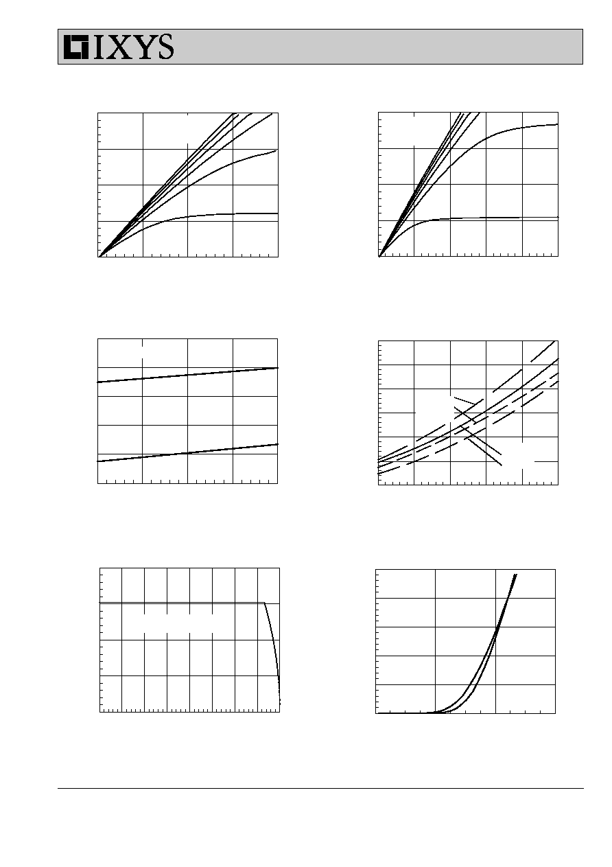
T
C
- Degrees C
-50 -25
0
25
50
75 100 125 150
I
D
- A
m
per
e
s
0
25
50
75
100
V
DS
- Volts
0
1
2
3
4
5
I
D
- A
m
per
e
s
0
50
100
150
200
V
GS
- Volts
2
4
6
8
I
D
- A
m
per
e
s
0
20
40
60
80
100
T
J
- Degrees C
25
50
75
100
125
150
R
DS
(
O
N)
-
No
r
m
a
liz
e
d
0.8
1.0
1.2
1.4
1.6
1.8
2.0
I
D
- Amperes
0
50
100
150
200
R
DS
(
O
N)
-
N
o
r
m
a
liz
e
d
0.8
1.0
1.2
1.4
1.6
1.8
V
DS
- Volts
0.0
0.5
1.0
1.5
2.0
I
D
- A
m
per
e
s
0
50
100
150
200
5V
V
GS
= 10V
V
GS
=10V
9V
8V
T
J
=125
O
C
T
J
=25
O
C
6V
6V
5V
T
J
= 25
o
C
I
D
=180A
T
J
= 25
O
C
T
J
= 125
o
C
V
GS
=10V
9V
8V
T
J
= 125
O
C
7V
7V
V
GS
=10V
V
GS
=15V
V
GS
=10V
V
GS
=15V
I
D
=90A
Lead Current Limit
IXF 180N10 P1
Figure 3. R
DS(on)
normalized to 15A/25
O
C vs. I
D
Figure 5. Drain Current vs. Case Temperature
Figure 6. Admittance Curves
Figure 1. Output Characteristics at 25
O
C
Figure 2. Output Characteristics at 125
O
C
Figure 4. R
DS(on)
normalized to 15A/25
O
C vs. T
J
IXFK 180N10
IXFX 180N10
4 - 4
© 2000 IXYS All rights reserved
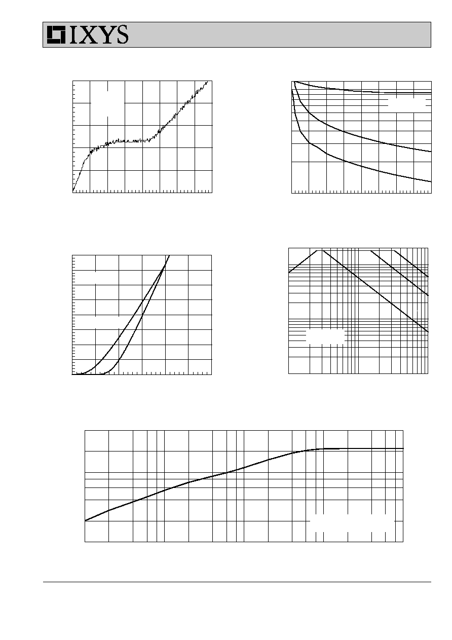
Pulse Width - Seconds
10
-3
10
-2
10
-1
10
0
10
1
R(th)
JC
- K
/
W
0.02
0.04
0.06
0.08
0.20
0.40
0.01
0.10
V
DS
- Volts
0
5
10
15
20
25
30
35
40
C
a
p
a
c
i
t
a
nc
e
-
pF
1000
10000
V
SD
- Volts
0.4
0.6
0.8
1.0
1.2
1.4
1.6
I
D
- A
m
p
e
r
e
s
0
25
50
75
100
125
150
175
200
Gate Charge - nC
0
50
100 150 200 250 300 350 400
V
GS
-
Vo
lt
s
0
3
6
9
12
15
Crss
Coss
Ciss
T
J
=25
O
C
V
DS
=50V
I
D
=90A
I
G
=10mA
F = 100kHz
V
DS
- Volts
1
10
100
I
D
- A
m
per
e
s
1
10
100
T
C
= 25
O
C
10 ms
1 ms
DC
200
V
GS
= 0V
T
J
=125
O
C
Figure 7. Gate Charge
Figure 8. Capacitance Curves
Figure 9. Forward Voltage Drop of the Intrinsic Diode
Figure 10. Forward Bias Safe Operating Area
Figure 11. Transient Thermal Resistance
R
i
:
0.02
0.046
0.154
t
i
:
0.007
0.01
0.25
R(th)
JC
=
S
R
i
{1-exp(-t/
t
i
)}
i=1
3
IXFK 180N10
IXFX 180N10