© 2002 IXYS All rights reserved
Symbol
Test Conditions
Characteristic Values
(T
J
= 25
∞
C, unless otherwise specified)
Min.
Typ.
Max.
BV
CES
I
C
= 250
µ
A, V
GE
= 0 V
600
V
V
GE(th)
I
C
= 250
µ
A, V
GE
= V
GE
2.5
5.0
V
I
CES
V
CE
= 0.8, V
CES
T
J
= 25
∞
C
200
µ
A
V
GE
= 0 V
T
J
= 125
∞
C
1
mA
I
GES
V
CE
= 0 V, V
GE
=
±
20 V
±
100
nA
V
CE(sat)
I
C
= I
CE90
, V
GE
= 15
2.1
2.7
V
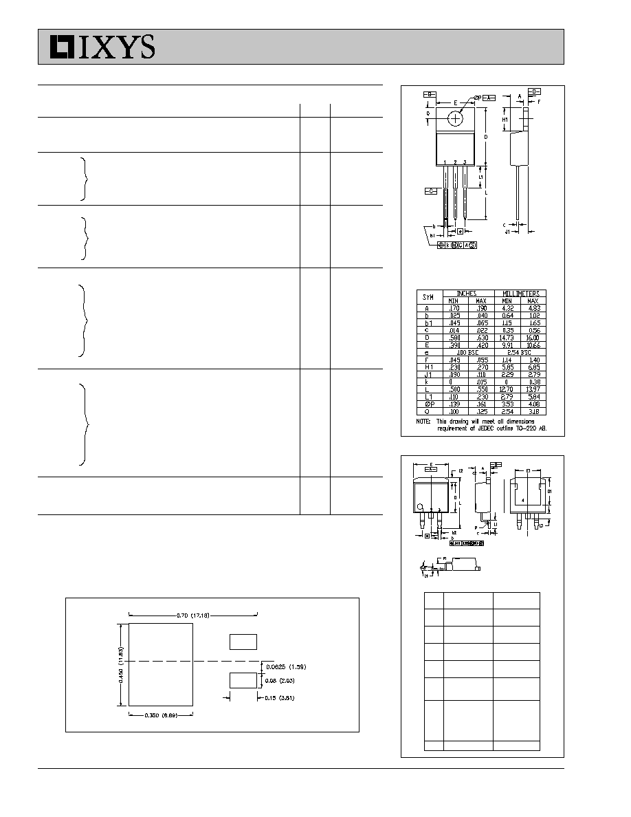
TO-220 AB
(IXGP)
C (tab)
TO-263 AA (IXGA)
Symbol
Test Conditions
Maximum Ratings
V
CES
T
J
= 25
∞
C to 150
∞
C
600
V
V
CGR
T
J
= 25
∞
C to 150
∞
C; R
GE
= 1 M
600
V
V
GES
Continuous
±
20
V
V
GEM
Transient
±
30
V
I
C25
T
C
= 25
∞
C
24
A
I
C90
T
C
= 90
∞
C
12
A
I
CM
T
C
= 25
∞
C, 1 ms
48
A
SSOA
V
GE
= 15 V, T
VJ
= 125
∞
C, R
G
= 33
I
CM
= 24
A
(RBSOA)
Clamped inductive load, L = 300
µ
H
@ 0.8 V
CES
P
C
T
C
= 25
∞
C
100
W
T
J
-55 ... +150
∞
C
T
JM
150
∞
C
T
stg
-55 ... +150
∞
C
M
d
Mounting torque with screw M3
0.45/4 Nm/lb.in.
Mounting torque with screw M3.5
0.55/5 Nm/lb.in.
Weight
4
g
Maximum lead temperature for soldering
300
∞
C
1.6 mm (0.062 in.) from case for 10 s
G = Gate
C
= Collector
E = Emitter
TAB = Collector
G
E
97534B (2/02)
HiPerFAST
TM
IGBT
Features
∑
Very high freqency IGBT
∑
New generation HDMOS
TM
process
∑
International standard package
JEDEC TO-220AB and TO-263AA
∑
High peak current handling capability
Applications
∑
PFC circuits
∑
AC motor speed control
∑
DC servo & robot drives
∑
Switch-mode and resonant-mode
power supplies
∑
High power audio amplifiers
Advantages
∑
Fast switching speed
∑
High power density
E
C
G
V
CES
= 600 V
I
C25
=
2
4
A
V
CE(sat)
= 2.7 V
t
fi(typ)
=
55 ns
IXGA 12N60C
IXGP 12N60C
IXYS reserves the right to change limits, test conditions, and dimensions.
IXYS MOSFETS and IGBTs are covered by one or more of the following U.S. patents:
4,835,592
4,881,106
5,017,508
5,049,961
5,187,117
5,486,715
6,306,728B1
4,850,072
4,931,844
5,034,796
5,063,307
5,237,481
5,381,025
IXGA12N60C IXGP12N60C
TO-263 AA Outline
1. Gate
2. Collector
3. Emitter
4. Collector
Bottom Side
Dim.
Millimeter
Inches
Min.
Max.
Min.
Max.
A
4.06
4.83
.160
.190
A1
2.03
2.79
.080
.110
b
0.51
0.99
.020
.039
b2
1.14
1.40
.045
.055
c
0.46
0.74
.018
.029
c2
1.14
1.40
.045
.055
D
8.64
9.65
.340
.380
D1
7.11
8.13
.280
.320
E
9.65
10.29
.380
.405
E1
6.86
8.13
.270
.320
e
2.54
BSC
.100
BSC
L
14.61
15.88
.575
.625
L1
2.29
2.79
.090
.110
L2
1.02
1.40
.040
.055
L3
1.27
1.78
.050
.070
L4
0
0.38
0
.015
R
0.46
0.74
.018
.029
Pins: 1 - Gate
2 - Collector
3 - Emitter
4 - Collector
Bottom Side
TO-220 AB Dimensions
Symbol
Test Conditions
Characteristic Values
(T
J
= 25
∞
C, unless otherwise specified)
Min. Typ.
Max.
g
fs
I
C
= I
C90
; V
CE
= 10 V,
7
11
S
Pulse test, t
300
µ
s, duty cycle
2 %
C
ies
860
pF
C
oes
V
CE
= 25 V, V
GE
= 0 V, f = 1 MHz
64
pF
C
res
15
pF
Q
g
32
nC
Q
ge
I
C
= I
C90
, V
GE
= 15 V, V
CE
= 0.5 V
CES
10
nC
Q
gc
10
nC
t
d(on)
20
ns
t
ri
20
ns
t
d(off)
60
ns
t
fi
55
ns
E
off
0.09
mJ
t
d(on)
20
ns
t
ri
20
ns
E
on
0.15
mJ
t
d(off)
85
180
ns
t
fi
85
180
ns
E
off
0.27
0.60
mJ
R
thJC
1.25
K/W
R
thCK
0.25
K/W
Inductive load, T
J
= 25
∞∞
∞∞
∞
C
I
C
= I
C90
, V
GE
= 15 V, L = 300
µ
H
V
CE
= 0.8 V
CES
, R
G
= R
off
= 18
Remarks: Switching
times
may
increase for V
CE
(Clamp) > 0.8 V
CES
,
higher T
J
or increased R
G
Min. Recommended Footprint
(Dimensions in inches and mm)
Inductive load, T
J
= 125
∞∞
∞∞
∞
C
I
C
= I
C90
, V
GE
= 15 V, L = 300
µ
H
V
CE
= 0.8 V
CES
, R
G
= R
off
= 18
Remarks: Switching times may
increase for V
CE
(Clamp) > 0.8 V
CES
,
higher T
J
or increased R
G

© 2002 IXYS All rights reserved
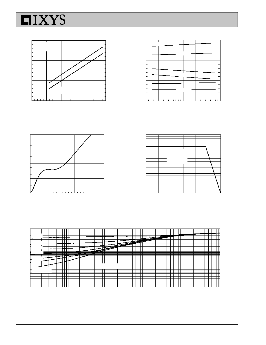
Fig. 2. Extended Output Characteristics
Fig. 1. Saturation Voltage Characteristics
Fig. 4. Temperature Dependence of V
CE(sat)
Fig. 3. Saturation Voltage Characteristics
Fig. 6. Junction Capacitance Curves
Fig. 5. Saturation Voltage Characteristics
V
CE
- Volts
0
2
4
6
8
10
I
C
- A
m
pe
re
s
0
10
20
30
40
50
V
CE
-Volts
0
5
10
15
20
25
30
35
40
C
a
pac
i
t
a
nce
-
pF
1
10
100
1000
T
J
- Degrees C
25
50
75
100
125
150
V
CE
(s
a
t
)
- N
o
rm
a
l
i
z
ed
0.50
0.75
1.00
1.25
1.50
1.75
V
CE
- Volts
0
2
4
6
8
10
I
C
- A
m
pe
re
s
0
10
20
30
40
50
V
GE
- Volts
3
4
5
6
7
8
9
10
I
C
- A
m
pe
re
s
0
5
10
15
20
25
30
13V
11V
9V
7V
V
CE
= 10V
V
GE
= 15V
T
J
= 25∞C
V
GE
= 15V
T
J
= 25∞C
I
C
= 6A
I
C
= 12A
I
C
= 24A
T
J
=
125∞C
f = 1Mhz
5V
5V
V
GE
= 15V
T
J
= 25∞C
T
J
= 125∞C
7V
9V
5V
9V
V
GE
= 15V
C
iss
C
oss
C
rss
7V
11V
11V
13V
13V
V
CE
- Volts
0
4
8
12
16
20
I
C
- A
m
pe
re
s
0
20
40
60
80
100
IXGA12N60C IXGP12N60C
IXYS reserves the right to change limits, test conditions, and dimensions.
IXYS MOSFETS and IGBTs are covered by one or more of the following U.S. patents:
4,835,592
4,881,106
5,017,508
5,049,961
5,187,117
5,486,715
6,306,728B1
4,850,072
4,931,844
5,034,796
5,063,307
5,237,481
5,381,025
IXGA12N60C IXGP12N60C
Fig. 11. Transient Thermal Resistance
Fig. 8. Dependence of E
ON
and E
OFF
on R
G
.
Fig. 7. Dependence of E
ON
and E
OFF
on I
C
.
Fig. 9. Gate Charge
Fig. 10. Turn-off Safe Operating Area
Pulse Width - Seconds
0.00001
0.0001
0.001
0.01
0.1
1
Z
th
J
C
(K
/W
)
0.001
0.01
0.1
1
V
CE
- Volts
0
100
200
300
400
500
600
I
C
-
A
m
p
e
res
0.1
1
10
100
Q
g
- nanocoulombs
0
10
20
30
40
50
V
GE
-
Vo
lt
s
0
4
8
12
16
R
G
- Ohms
0
10
20
30
40
50
60
E
(O
F
F
)
-
m
i
lli
jo
u
l
es
0
1
2
3
E
(O
N)
-
m
i
ll
ij
ou
le
s
0.0
0.5
1.0
1.5
I
C
- Amperes
0
5
10
15
20
25
E
(O
F
F
)
-
m
i
ll
iJ
ou
le
s
0
1
2
3
E
(O
N)
-
m
i
lli
jo
u
l
es
0.0
0.5
1.0
1.5
V
CE
= 300V
I
C
= 6A
I
C
= 12A
E
(ON)
E
(OFF)
T
J
= 125∞C
R
G
= 4.7
dV/dt < 5V/ns
D=0.5
D=0.1
D=0.05
D=0.01
Single pulse
D = Duty Cycle
R
G
= 10
T
J
= 125∞C
24
E
(ON)
I
C
=24A
E
(OFF)
T
J
= 125∞C
E
(ON)
I
C
= 12A
E
(ON)
E
(OFF)
E
(OFF)
D=0.2
D=0.02