© 2003 IXYS All rights reserved
HiPerFAST
TM
IGBT
with Diode
Lightspeed
TM
Series
Symbol
Test Conditions
Maximum Ratings
V
CES
T
J
= 25∞C to 150∞C
600
V
V
CGR
T
J
= 25∞C to 150∞C; R
GE
= 1 M
600
V
V
GES
Continuous
±20
V
V
GEM
Transient
±30
V
I
C25
T
C
= 25∞C
14
A
I
C90
T
C
= 90∞C
7
A
I
CM
T
C
= 25∞C, 1 ms
30
A
SSOA
V
GE
= 15 V, T
VJ
= 125∞C, R
G
= 22
I
CM
= 14
A
(RBSOA)
Clamped inductive load, L = 300
µ
H
@ 0.8 V
CES
P
C
T
C
= 25∞C
75
W
T
J
-55 ... +150
∞C
T
JM
150
∞C
T
stg
-55 ... +150
∞C
Maximum lead temperature for soldering
300
∞C
1.6 mm (0.062 in.) from case for 10 s
M
d
Mounting torque, (TO-220) M3
0.45/4 Nm/lb.in.
M3.5
0.55/5 Nm/lb.in.
Weight
TO-220
4
g
TO-263
2
g
Symbol
Test Conditions
Characteristic Values
(T
J
= 25∞C, unless otherwise specified)
min.
typ.
max.
BV
CES
I
C
= 250
µ
A, V
GE
= 0 V
600
V
V
GE(th)
I
C
= 250
µ
A, V
CE
= V
GE
2.5
5.5
V
I
CES
V
CE
= 0.8 ∑ V
CES
T
J
= 25∞C
100
µ
A
V
GE
= 0 V
T
J
= 125∞C
750
µ
A
I
GES
V
CE
= 0 V, V
GE
= ±20 V
±100
nA
V
CE(sat)
I
C
= I
C90
, V
GE
= 15 V
2.0
2.5
V
Features
∑
International standard packages
JEDEC TO-263 surface
mountable and JEDEC TO-220 AB
∑
High frequency IGBT
∑
High current handling capability
∑
HiPerFAST
TM
HDMOS
TM
process
∑
MOS Gate turn-on
- drive simplicity
Applications
∑
Uninterruptible power supplies (UPS)
∑
Switched-mode and resonant-mode
power supplies
∑
AC motor speed control
∑
DC servo and robot drives
∑
DC choppers
Advantages
∑
High power density
∑
Suitable for surface mounting
∑
Very low switching losses for high
frequency applications
V
CES
= 600 V
I
C25
= 14 A
V
CE(sat)typ
= 2.0 V
t
fi
= 45 ns
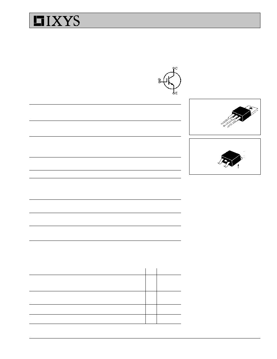
G = Gate,
C = Collector,
E = Emitter,
TAB = Collector
G
E
C (TAB)
TO-263 AA (IXGA)
G C
E
TO-220AB (IXGP)
DS98720A(01/03)
IXGA 7N60CD1
IXGP 7N60CD1
Preliminary Data
IXYS reserves the right to change limits, test conditions, and dimensions.
IXYS MOSFETs and IGBTs are covered by one or more of the following U.S. patents:
4,835,592
4,881,106
5,017,508
5,049,961
5,187,117
5,486,715
6,306,728B1
4,850,072
4,931,844
5,034,796
5,063,307
5,237,481
5,381,025
IXGA 7N60CD1
IXGP 7N60CD1
Symbol
Test Conditions
Characteristic Values
(T
J
= 25
∞
C, unless otherwise specified)
min.
typ.
max.
g
fs
I
C
= I
C90
; V
CE
= 10 V,
3
7
S
Pulse test, t
300
µ
s, duty cycle
2 %
C
ies
500
pF
C
oes
V
CE
= 25 V, V
GE
= 0 V, f = 1 MHz
50
pF
C
res
17
pF
Q
g
25
nC
Q
ge
I
C
= I
C90
, V
GE
= 15 V, V
CE
= 0.5 V
CES
15
nC
Q
gc
10
nC
t
d(on)
10
ns
t
ri
10
ns
t
d(off)
65
130
ns
t
fi
45
110
ns
E
off
0.12
0.25
mJ
t
d(on)
10
ns
t
ri
15
ns
E
on
0.15
mJ
t
d(off)
120
ns
t
fi
85
ns
E
off
0.22
mJ
R
thJC
IGBT
1.65 K/W
R
thCK
0.25
K/W
Inductive load, T
J
= 25
∞∞
∞∞
∞
C
I
C
= I
C90
, V
GE
= 15 V, L = 300
µ
H
V
CE
= 0.8 ∑ V
CES
, R
G
= R
off
= 18
Remarks: Switching times may increase
for V
CE
(Clamp) > 0.8 ∑ V
CES
, higher T
J
or
increased R
G
Inductive load, T
J
= 125
∞∞
∞∞
∞
C
I
C
= I
C90
, V
GE
= 15 V, L = 300
µ
H
V
CE
= 0.8 ∑ V
CES
, R
G
= R
off
= 18
Remarks: Switching times may increase
for V
CE
(Clamp) > 0.8 ∑ V
CES
, higher T
J
or
increased R
G
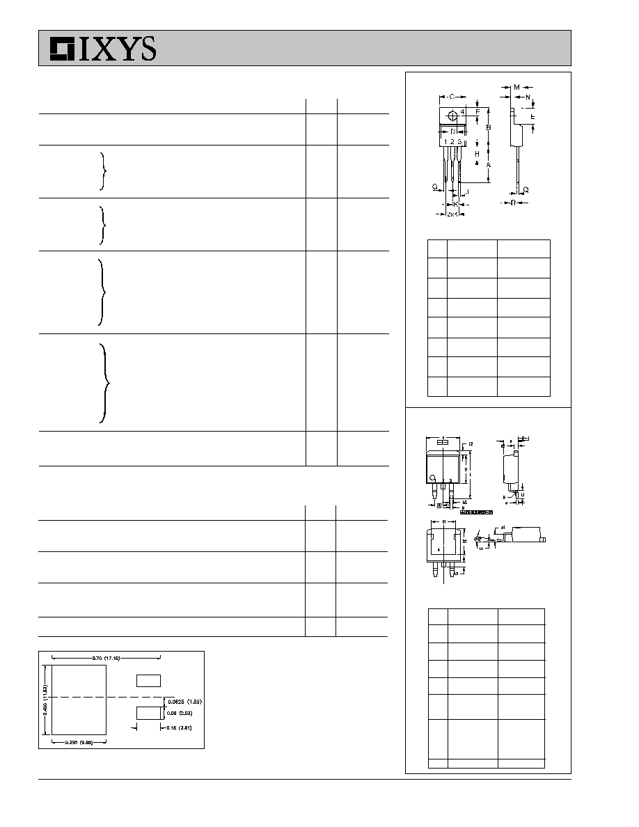
TO-220 AB Outline
Dim.
Millimeter
Inches
Min.
Max.
Min.
Max.
A
12.70
13.97
0.500
0.550
B
14.73
16.00
0.580
0.630
C
9.91
10.66
0.390
0.420
D
3.54
4.08
0.139
0.161
E
5.85
6.85
0.230
0.270
F
2.54
3.18
0.100
0.125
G
1.15
1.65
0.045
0.065
H
2.79
5.84
0.110
0.230
J
0.64
1.01
0.025
0.040
K
2.54
BSC
0.100
BSC
M
4.32
4.82
0.170
0.190
N
1.14
1.39
0.045
0.055
Q
0.35
0.56
0.014
0.022
R
2.29
2.79
0.090
0.110
1. Gate
2. Collector
3. Emitter
4. Collector
Botton Side
Dim.
Millimeter
Inches
Min.
Max.
Min.
Max.
A
4.06
4.83
.160
.190
A1
2.03
2.79
.080
.110
b
0.51
0.99
.020
.039
b2
1.14
1.40
.045
.055
c
0.46
0.74
.018
.029
c2
1.14
1.40
.045
.055
D
8.64
9.65
.340
.380
D1
7.11
8.13
.280
.320
E
9.65
10.29
.380
.405
E1
6.86
8.13
.270
.320
e
2.54
BSC
.100
BSC
L
14.61
15.88
.575
.625
L1
2.29
2.79
.090
.110
L2
1.02
1.40
.040
.055
L3
1.27
1.78
.050
.070
L4
0
0.38
0
.015
R
0.46
0.74
.018
.029
TO-263 AA Outline
Pins:
1 - Gate
2 - Collector
3 - Emitter
4 - Collector
Bottom Side
Reverse Diode (FRED)
Characteristic Values
(T
J
= 25
∞
C, unless otherwise specified)
Symbol
Test Conditions
min.
typ.
max.
V
F
I
F
= 10A; T
VJ
= 150
∞
C
1.96
V
T
VJ
= 25
∞
C
2.95
V
I
RM
V
R
= 100 V; I
F
=25A; -di
F
/dt = 100 A/
µ
s
2
2.5
V
L < 0.05
µ
H
; T
VJ
= 100
∞
C
t
rr
I
F
= 1 A; -di/dt = 50 A/
µ
s;
V
R
= 30 V T
J
= 25
∞
C
35
ns
R
thJC
Diode
1.6 K/W
Min. Recommended Footprint
(Dimensions in inches and mm)