
© 2002 IXYS All rights reserved
HiPerFAST
TM
IGBT
V
CES
= 1200 V
I
C25
= 30 A
V
CE(sat)
= 3.2 V
t
fi(typ)
= 160 ns
IXGH 15N120B
IXGT 15N120B
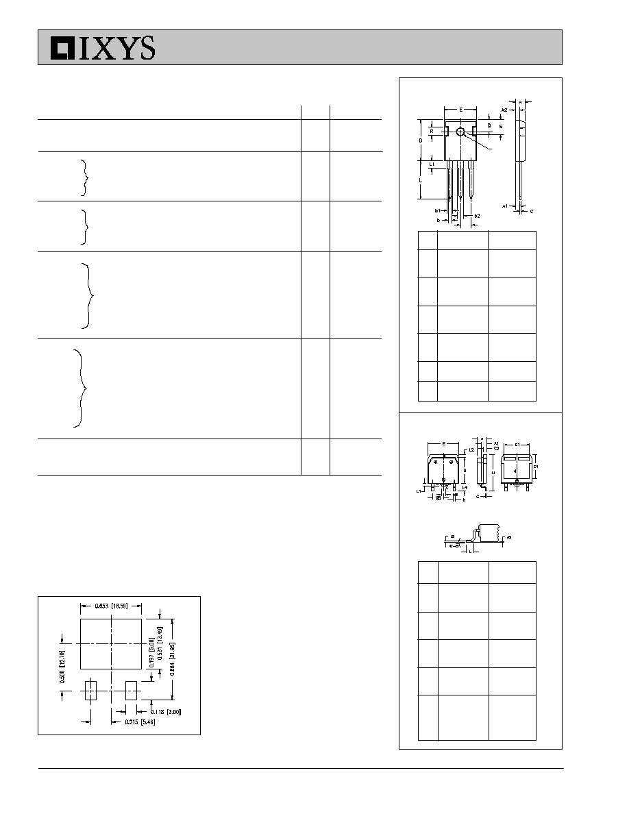
C (TAB)
G = Gate,
C = Collector,
E = Emitter,
TAB = Collector
G
C
E
TO-247 AD (IXGH)
Features
International standard packages
JEDEC TO-268 surface and
JEDEC TO-247 AD
Low switching losses, low V
(sat)
MOS Gate turn-on
- drive simplicity
Applications
AC motor speed control
DC servo and robot drives
DC choppers
Uninterruptible power supplies (UPS)
Switched-mode and resonant-mode
power supplies
Advantages
High power density
Suitable for surface mounting
Easy to mount with 1 screw,
(isolated mounting screw hole)
98659-A (7-02)
Symbol
Test Conditions
Characteristic Values
(T
J
= 25
∞C, unless otherwise specified)
min.
typ.
max.
BV
CES
I
C
= 250
µA, V
GE
= 0 V
1200
V
V
GE(th)
I
C
= 250
µA, V
CE
= V
GE
2.5
5
V
I
CES
V
CE
= V
CES
T
J
= 25
∞C
100
µA
V
GE
= 0 V
T
J
= 125
∞C
3.5
mA
I
GES
V
CE
= 0 V, V
GE
=
±20 V
±100
nA
V
CE(sat)
I
C
= I
C90
, V
GE
= 15 V
3.2
V
T
J
= 125
∞C
2.5
V
Symbol
Test Conditions
Maximum Ratings
V
CES
T
J
= 25
∞C to 150∞C
1200
V
V
CGR
T
J
= 25
∞C to 150∞C; R
GE
= 1 M
1200
V
V
GES
Continuous
±20
V
V
GEM
Transient
±30
V
I
C25
T
C
= 25
∞C
30
A
I
C90
T
C
= 90
∞C
15
A
I
CM
T
C
= 25
∞C, 1 ms
60
A
SSOA
V
GE
= 15 V, T
VJ
= 125
∞C, R
G
= 10
I
CM
= 40
A
(RBSOA)
Clamped inductive load
@ 0.8 V
CES
P
C
T
C
= 25
∞C
150
W
T
J
-55 ... +150
∞C
T
JM
150
∞C
T
stg
-55 ... +150
∞C
Maximum Lead temperature for soldering
300
∞C
1.6 mm (0.062 in.) from case for 10 s
Maximum Tab temperature for soldering SMD devices for 10 s
260
∞C
M
d
Mounting torque (M3)
1.13/10Nm/lb.in.
Weight
TO-247 AD
6
g
TO-268
4
g
TO-268 (IXGT)
G
E
C (TAB)
IXYS reserves the right to change limits, test conditions, and dimensions.
IXYS MOSFETS and IGBTs are covered by one or more of the following U.S. patents:
4,835,592
4,881,106
5,017,508
5,049,961
5,187,117
5,486,715
6,306,728B1
4,850,072
4,931,844
5,034,796
5,063,307
5,237,481
5,381,025
Dim.
Millimeter
Inches
Min.
Max.
Min. Max.
A
4.7
5.3
.185
.209
A
1
2.2
2.54
.087
.102
A
2
2.2
2.6
.059
.098
b
1.0
1.4
.040
.055
b
1
1.65
2.13
.065
.084
b
2
2.87
3.12
.113
.123
C
.4
.8
.016
.031
D
20.80
21.46
.819
.845
E
15.75
16.26
.610
.640
e
5.20
5.72
0.205 0.225
L
19.81
20.32
.780
.800
L1
4.50
.177
P
3.55
3.65
.140
.144
Q
5.89
6.40
0.232 0.252
R
4.32
5.49
.170
.216
S
6.15 BSC
242 BSC
e
P
TO-247 AD Outline
Remarks: Switching times may
increase for V
CE
(Clamp) > 0.8 ∑ V
CES
,
higher T
J
or increased R
G
Remarks: Switching times may
increase for V
CE
(Clamp) > 0.8 ∑ V
CES
,
higher T
J
or increased R
G
Symbol
Test Conditions
Characteristic Values
(T
J
= 25
∞C, unless otherwise specified)
min.
typ.
max.
g
fs
I
C
= I
C90
; V
CE
= 10 V,
12
15
S
Pulse test, t
300 µs, duty cycle 2 %
C
ies
1720
pF
C
oes
V
CE
= 25 V, V
GE
= 0 V, f = 1 MHz
95
pF
C
res
35
pF
Q
g
69
nC
Q
ge
I
C
= I
C90
, V
GE
= 15 V, V
CE
= 0.5 V
CES
13
nC
Q
gc
26
nC
t
d(on)
25
ns
t
ri
15
ns
t
d(off)
180
280
ns
t
fi
160
320
ns
E
off
1.75
3.0 mJ
t
d(on)
25
ns
t
ri
18
ns
E
on
0.60
mJ
t
d(off)
300
ns
t
fi
360
ns
E
off
3.5
mJ
R
thJC
0.83 K/W
R
thCK
(TO-247)
0.25
K/W
Inductive load, T
J
= 125
∞∞
∞∞
∞C
I
C
= I
C90
, V
GE
= 15 V
V
CE
= 0.8 V
CES
, R
G
= R
off
= 10
Inductive load, T
J
= 25
∞∞
∞∞
∞C
I
C
= I
C90
, V
GE
= 15 V
V
CE
= 0.8 V
CES
, R
G
= R
off
= 10
Min Recommended Footprint
IXGH 15N120B
IXGT 15N120B
TO-268 Outline
Dim.
Millimeter
Inches
Min.
Max.
Min. Max.
A
4.9
5.1
.193
.201
A
1
2.7
2.9
.106
.114
A
2
.02
.25
.001
.010
b
1.15
1.45
.045
.057
b
2
1.9
2.1
.75
.83
C
.4
.65
.016
.026
D
13.80
14.00
.543
.551
E
15.85
16.05
.624
.632
E
1
13.3
13.6
.524
.535
e 5.45 BSC .215 BSC
H
18.70
19.10
.736
.752
L
2.40
2.70
.094
.106
L1
1.20
1.40
.047
.055
L2
1.00
1.15
.039
.045
L3 0.25 BSC .010 BSC
L4
3.80
4.10
.150
.161
© 2002 IXYS All rights reserved
IXGH 15N120B
IXGT 15N120B
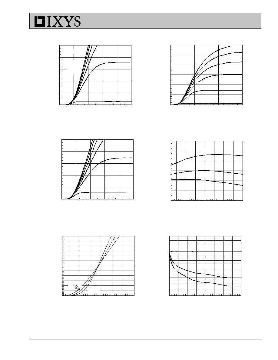
V
CE
- Volts
0
2
4
6
8
10
I
C
- A
m
p
e
r
e
s
0
10
20
30
40
50
5V
T
J
= 25
O
C
7V
V
GS
= 15V
13V
11V
IXG_15N120B-P1
9V
V
GE
= 15V
T
J
- Degrees C
-25
0
25
50
75
100 125 150
V
CE
(S
A
T
)
-
N
o
r
m
a
liz
e
d
0.4
0.6
0.8
1.0
1.2
1.4
1.6
I
C
= 30A
I
C
= 15A
I
C
= 7.5A
V
CE
- Volts
0
5
10
15
I
C
- A
m
p
e
r
e
s
0
25
50
75
100
125
150
T
J
= 25
o
C
13V
V
GE
= 15V
11V
9V
7V
5V
V
CE
- Volts
0
5
10
15
20
25
30
35
40
C
a
pa
c
i
t
a
nc
e
-
pF
10
100
1000
10000
V
GE
- Volts
4
5
6
7
8
9
10
I
C
-
A
m
p
e
r
e
s
0
5
10
15
20
25
30
35
40
45
50
55
60
T
J
= 125
o
C
T
J
= 25
o
C
T
J
= -40
o
C
V
CE
- Volts
0
2
4
6
8
10
I
C
- A
m
pe
r
e
s
0
10
20
30
40
50
T
J
= 125
O
C
5V
7V
V
GS
= 15V
13V
11V
9V
Fig. 1. Saturation Voltage Characteristics @ 25
o
C
Fig. 3. Saturation Voltage Characteristics @ 125
o
C
Fig. 5. Admittance Curves
Fig. 2. Extended Output Characteristics
Fig. 4. Temperature Dependence of VCE(sat)
Fig. 6. Capacitance Curves
IXYS reserves the right to change limits, test conditions, and dimensions.
IXYS MOSFETS and IGBTs are covered by one or more of the following U.S. patents:
4,835,592
4,881,106
5,017,508
5,049,961
5,187,117
5,486,715
6,306,728B1
4,850,072
4,931,844
5,034,796
5,063,307
5,237,481
5,381,025
IXGH 15N120B
IXGT 15N120B
Pulse Width - Seconds
0.00001
0.0001
0.001
0.01
0.1
1
Z
th
J
C
(
K
/W
)
0.001
0.01
0.1
1
D=0.2
V
CE
- Volts
0
200
400
600
800
1000 1200
I
C
-
A
m
p
e
re
s
0.1
1
10
100
Q
g
- nanocoulombs
0
10
20
30
40
50
V
GE
-
Vo
lts
0
2
4
6
8
10
12
14
16
R
G
- Ohms
0
10
20
30
40
50
60
E
(O
F
F
)
-
m
illi
jo
u
l
e
s
0
1
2
3
4
5
6
7
8
I
C
- Amperes
5
10
15
20
25
30
35
E
(O
F
F
)
-
m
ill
ij
ou
le
s
0
1
2
3
4
5
6
7
8
V
CE
= 600V
I
C
= 15A
T
J
= -55 to +125∞C
R
G
= 10
dV/dt < 5V/ns
D=0.5
D=0.1
D=0.05
D=0.02
D=0.01
Single pulse
IXGH15N120B-P2
D = Duty Cycle
R
G
= 10
T
J
= 125∞C
30
T
J
= 125∞C
I
C
= 15A
E
(OFF)
I
C
= 7.5A
I
C
= 30A
E
(OFF)
E
(OFF)
E
(OFF)
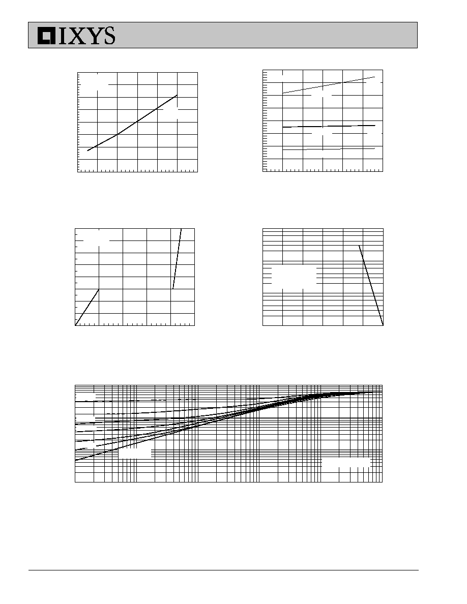
Fig. 7. Dependence of tfi and E
OFF
on I
C.
Fig. 8. Dependence of tfi and E
OFF
on R
G
.
Fig. 9. Gate Charge
Fig. 10. Turn-off Safe Operating Area
Fig. 11. Transient Thermal Resistance