© 2005 IXYS All rights reserved
DS99041C(10/05)
Symbol
Test Conditions
Characteristic Values
(T
J
= 25
∞C unless otherwise specified)
min.
typ.
max.
V
GE(th)
I
C
= 250
A, V
CE
= V
GE
3.0
5.0
V
I
CES
V
CE
= V
CES
T
J
= 25
∞C
200
A
V
GE
= 0 V
T
J
= 125
∞C
3
mA
I
GES
V
CE
= 0 V, V
GE
=
±20 V
±100
nA
V
CE(sat)
I
C
= I
C90
, V
GE
= 15 V
T
J
= 25
∞C
2.2
2.7
V
T
J
= 125
∞C
2.0
V
Symbol
Test Conditions
Maximum Ratings
V
CES
T
J
= 25
∞C to 150∞C
600
V
V
CGR
T
J
= 25
∞C to 150∞C; R
GE
= 1 M
600
V
V
GES
Continuous
±20
V
V
GEM
Transient
±30
V
I
C25
T
C
= 25
∞C (limited by leads)
75
A
I
C110
T
C
= 110
∞C
40
A
I
CM
T
C
= 25
∞C, 1 ms
200
A
SSOA
V
GE
= 15 V, T
VJ
= 125
∞C, R
G
= 10
I
CM
= 80
A
(RBSOA)
Clamped inductive load @ V
CE
600 V
P
C
T
C
= 25
∞C
300
W
T
J
-55 ... +150
∞C
T
JM
150
∞C
T
stg
-55 ... +150
∞C
Maximum Lead and Tab temperature for soldering
300
∞C
1.6 mm (0.062 in.) from case for 10 s
Plastic body
260
∞C
M
d
Mounting torque (IXGH)
1.13/10
Nm/lb.in
F
C
Mounting force (IXGJ)
20..120/4.5..25
N/lb
Weight
TO-247
6
g
TO-268 types
4
g
HiPerFAST
TM
IGBT
with Diode
Features
Very high frequency IGBT
Square RBSOA
High current handling capability
MOS Gate turn-on
- drive simplicity
Applications
Uninterruptible power supplies (UPS)
Switched-mode and resonant-mode
power supplies
AC motor speed control
DC servo and robot drives
DC choppers
Advantages
High power density
Very fast switching speeds for high
frequency applications
High power surface mountable
packages
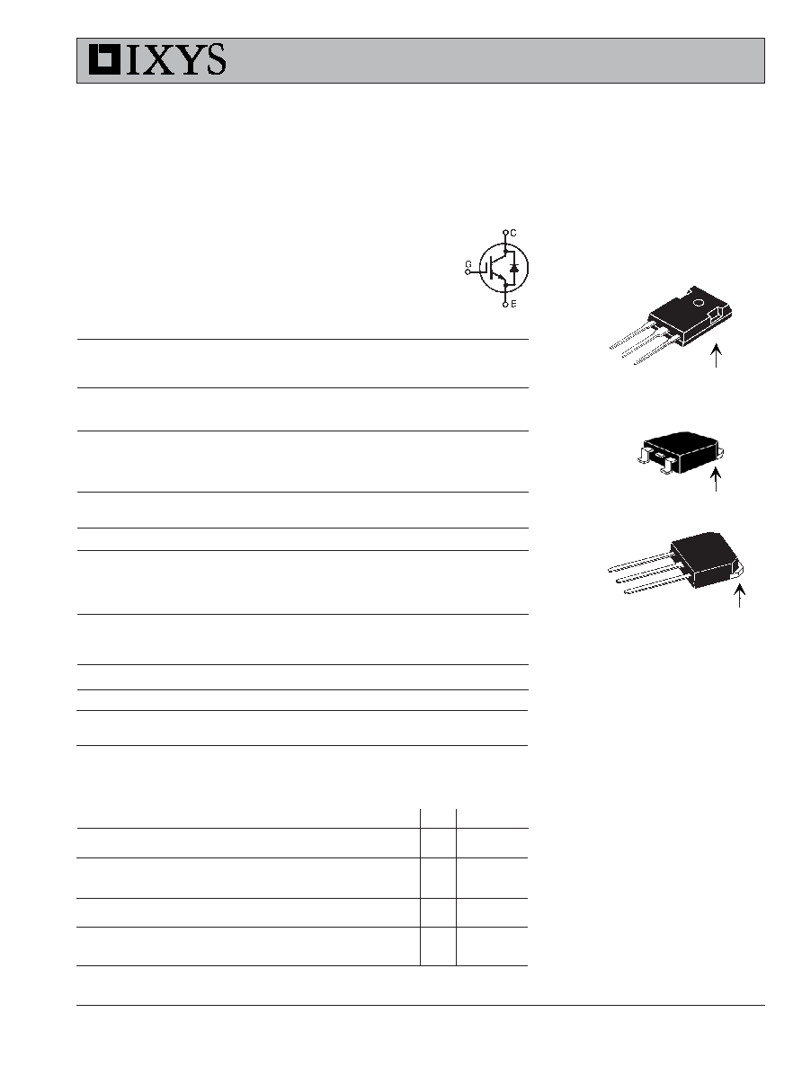
G = Gate
C = Collector
E = Emitter
G
C
E
TO-247(IXGH)
C (TAB)
TO-268 (D3) ( IXGT)
G
E
G
C
E
C (TAB)
C (TAB)
TO-268 Leaded ( IXGJ)
IXGH 40N60C2D1
IXGT 40N60C2D1
IXGJ 40N60C2D1
C2-Class High Speed IGBTs
V
CES
= 600
V
I
C25
= 56
A
V
CE(SAT)
= 2.7
V
t
fi(typ
= 32 ns
IXYS reserves the right to change limits, test conditions, and dimensions.
TO-247 AD Outline
Dim.
Millimeter
Inches
Min.
Max.
Min.
Max.
A
4.7
5.3
.185
.209
A
1
2.2
2.54
.087
.102
A
2
2.2
2.6
.059
.098
b
1.0
1.4
.040
.055
b
1
1.65
2.13
.065
.084
b
2
2.87
3.12
.113
.123
C
.4
.8
.016
.031
D
20.80
21.46
.819
.845
E
15.75
16.26
.610
.640
e
5.20
5.72
0.205 0.225
L
19.81
20.32
.780
.800
L1
4.50
.177
P
3.55
3.65
.140
.144
Q
5.89
6.40
0.232 0.252
R
4.32
5.49
.170
.216
S
6.15 BSC
242 BSC
e
P
Symbol
Test Conditions
Characteristic Values
(T
J
= 25
∞C unless otherwise specified)
min.
typ.
max.
g
fs
I
C
= 30 A; V
CE
= 10 V,
20
36
S
Pulse test, t
300 s, duty cycle 2 %
C
ies
2500
pF
C
oes
V
CE
= 25 V, V
GE
= 0 V, f = 1 MHz
220
pF
C
res
54
pF
Q
g
95
nC
Q
ge
I
C
= 30 A, V
GE
= 15 V, V
CE
= 0.5 V
CES
14
nC
Q
gc
36
nC
t
d(on)
18
n s
t
ri
20
n s
t
d(off)
90
140
n s
t
fi
32
n s
E
off
0.20
0.37 mJ
t
d(on)
18
n s
t
ri
20
n s
E
on
0.6
mJ
t
d(off)
130
n s
t
fi
80
240
n s
E
off
0.50
mJ
R
thJC
0.42 K/W
R
thCK
(IXGH, IXGJ )
0.25
K/W
Reverse Diode (FRED)
Characteristic Values
(T
J
= 25
∞C, unless otherwise specified)
Symbol
Test Conditions
min.
typ.
max.
V
F
I
F
= 30 A, V
GE
= 0 V, Pulse test T
J
=150
∞C
1.6
V
t
300 s, duty cycle d 2 % T
J
= 25
∞C
2.5
V
I
RM
I
F
= 30 A, V
GE
= 0 V, -di
F
/dt =100 A/
s, T
J
= 100
∞C
4
A
t
rr
V
R
= 100 V
T
J
= 100
∞C 100
n s
I
F
= 1 A; -di/dt = 100 A/
s; V
R
= 30 V
25
n s
R
thJC
0.9 K/W
Inductive load, T
J
= 25
∞∞
∞∞
∞C
I
C
= 30 A, V
GE
= 15 V
V
CE
= 400 V, R
G
= R
off
= 3
Inductive load, T
J
= 125
∞∞
∞∞
∞C
I
C
= 30 A, V
GE
= 15 V
V
CE
= 400 V, R
G
= R
off
= 3
IXGH 40N60C2D1 IXGT 40N60C2D1
IXGJ 40N60C2D1
TO-268 Outline
Terminals: 1 - Gate
2 - Collector
3 - Emitter
TO-268 Leaded Outline
IXYS MOSFETs and IGBTs are covered by
4,835,592
4,931,844
5,049,961
5,237,481
6,162,665
6,404,065 B1
6,683,344
6,727,585
one or more of the following U.S. patents:
4,850,072
5,017,508
5,063,307
5,381,025
6,259,123 B1
6,534,343
6,710,405B2
6,759,692
4,881,106
5,034,796
5,187,117
5,486,715
6,306,728 B1
6,583,505
6,710,463
6771478 B2

© 2005 IXYS All rights reserved
IXGH 40N60C2D1 IXGT 40N60C2D1
IXGJ 40N60C2D1
Fig. 2. Extended Output Characteristics
@ 25 deg. C
0
30
60
90
120
150
180
210
0
1
2
3
4
5
6
7
V
C E
- Volts
I
C
-
A
m
per
e
s
V
G E
= 1 5V
1 3V
1 1 V
9V
5V
7V
Fig. 3. Output Characteristics
@ 125 Deg. C
0
10
20
30
40
50
60
0.5
1
1.5
2
2.5
3
V
CE
- Volts
I
C
- A
m
p
e
re
s
V
G E
= 1 5V
1 3V
1 1 V
5V
7V
9V
Fig. 1. Output Characteristics
@ 25 Deg. C
0
10
20
30
40
50
60
0.5
1
1.5
2
2.5
3
3.5
V
C E
- Volts
I
C
-
A
m
p
e
re
s
V
G E
= 1 5V
1 3V
1 1 V
7V
5V
9V
Fig. 6. Input Admittance
0
30
60
90
120
150
180
210
4
5
6
7
8
9
10
V
G E
- Volts
I
C
-
A
m
per
es
T
J
= 1 25
∫
C
25
∫
C
-40
∫
C
Fig. 4. Temperature Dependence of V
CE(sat)
0.6
0.7
0.8
0.9
1
1.1
1.2
1.3
25
50
75
100
125
150
T
J
- Degrees Centigrade
V
C E
(s
a
t
)
- N
o
rm
a
l
i
z
e
d
I
C
= 60A
I
C
= 30A
I
C
= 1 5A
V
G E
= 1 5V
Fig. 5. Collector-to-Emitter Voltage
vs. Gate-to-Emitter voltage
1
1.5
2
2.5
3
3.5
4
5
6
7
8
9
10
11
12
13
14
15
V
G E
- Volts
V
C E
-
V
o
l
t
s
T
J
= 25
∫
C
I
C
= 60A
30A
1 5A
IXYS reserves the right to change limits, test conditions, and dimensions.
IXGH 40N60C2D1 IXGT 40N60C2D1
IXGJ 40N60C2D1
Fig. 12. Capacitance
10
100
1000
10000
0
5
10
15
20
25
30
35
40
V
C E
- Volts
Ca
pac
i
t
anc
e
-
p F
Cies
Coes
Cres
f = 1 M Hz
Fig. 11. Gate Charge
0
3
6
9
12
15
0
20
40
60
80
100
Q
G
- nanoCoulombs
V
G E
-
V
o
l
t
s
V
C E
= 300V
I
C
= 30A
I
G
= 1 0mA
Fig. 7. Transconductance
0
10
20
30
40
50
60
70
0
30
60
90
120
150
180
I
C
- Amperes
g
f s
-
S
i
em
ens
T
J
= -40
∫
C
25
∫
C
1 25
∫
C
Fig. 8. Dependence of E
off
on R
G
0
0.2
0.4
0.6
0.8
1
1.2
1.4
1.6
1.8
2
4
6
8
10
12
14
16
R
G
- Ohms
E
o
ff
-
m
illiJ
o
u
l
e
s
I
C
= 45A
I
C
= 1 5A
T
J
= 1 25
∫
C
V
G E
= 1 5V
V
C E
= 400V
I
C
= 30A
I
C
= 60A
Fig. 10. Dependence of E
off
on Temperature
0
0.2
0.4
0.6
0.8
1
1.2
1.4
1.6
25
50
75
100
125
T
J
- Degrees Centigrade
E
of
f
-
m
illiJ
ou
le
s
I
C
= 60A
V
G E
= 1 5V
V
C E
= 400V
R
G
= 3 Ohms
R
G
= 1 0 Ohms
- - - - -
I
C
= 45A
I
C
= 30A
I
C
= 1 5A
Fig. 9. Dependence of E
off
on I
C
0
0.2
0.4
0.6
0.8
1
1.2
1.4
1.6
10
20
30
40
50
60
I
C
- Amperes
E
of
f
-
M
illiJ
o
u
l
e
s
R
G
= 3 Ohms
R
G
= 1 0 Ohms
- - - - -
V
G E
= 1 5V
V
C E
= 400V
T
J
= 1 25
∫
C
T
J
= 25
∫
C
© 2005 IXYS All rights reserved
200
600
1000
0
400
800
60
70
80
90
0.00001
0.0001
0.001
0.01
0.1
1
0.001
0.01
0.1
1
0
40
80
120
160
0.0
0.5
1.0
1.5
2.0
K
f
T
VJ
∞C
-di
F
/dt
t
s
K/W
0
200
400
600
800
1000
0
5
10
15
20
0.00
0.25
0.50
0.75
1.00
V
FR
di
F
/dt
V
200
600
1000
0
400
800
0
5
10
15
20
25
30
100
1000
0
200
400
600
800
1000
0
1
2
3
0
10
20
30
40
50
60
I
RM
Q
r
I
F
A
V
F
-di
F
/dt
-di
F
/dt
A/
s
A
V
nC
A/
s
A/
s
t
rr
ns
t
fr
Z
thJC
A/
s
s
DSEP 29-06
I
F
= 60A
I
F
= 30A
I
F
= 15A
T
VJ
= 100∞C
V
R
= 300V
T
VJ
= 100∞C
I
F
= 30A
Fig. 14 Peak reverse current I
RM
versus -di
F
/dt
Fig. 13 Reverse recovery charge Q
r
versus -di
F
/dt
Fig. 12 Forward current I
F
versus V
F
T
VJ
= 100∞C
V
R
= 300V
T
VJ
= 100∞C
V
R
= 300V
I
F
= 60A
I
F
= 30A
I
F
= 15A
Q
r
I
RM
Fig. 15 Dynamic parameters Q
r
, I
RM
versus T
VJ
Fig. 16 Recovery time t
rr
versus -di
F
/dt
Fig. 17 Peak forward voltage V
FR
and
t
fr
versus di
F
/dt
I
F
= 60A
I
F
= 30A
I
F
= 15A
t
fr
V
FR
Fig. 18 Transient thermal resistance junction to case
Constants for Z
thJC
calculation:
i
R
thi
(K/W)
t
i
(s)
1
0.502
0.0052
2
0.193
0.0003
3
0.205
0.0162
T
VJ
=25∞C
T
VJ
=100∞C
T
VJ
=150∞C
IXGH 40N60C2D1 IXGT 40N60C2D1
IXGJ 40N60C2D1