© 2004 IXYS All rights reserved
V
CES
= 900 V
I
C25
= 75 A
V
CE(sat)
= 2.7 V
t
fi
typ
= 200 ns
Symbol
Test Conditions
Characteristic Values
(T
J
= 25
∞C, unless otherwise specified)
min.
typ. max.
V
GE(th)
I
C
= 250
µA, V
CE
= V
GE
3.0
5.0
V
I
CES
V
CE
= V
CES
T
J
= 25
∞C
50
µA
V
GE
= 0 V
T
J
= 150
∞C
1
mA
I
GES
V
CE
= 0 V, V
GE
=
±20 V
±100
nA
V
CE(sat)
I
C
= I
C110
, V
GE
= 15 V
2.2
2.7
V
T
J
= 125
∞C
V
Symbol
Test Conditions
Maximum Ratings
V
CES
T
J
= 25
∞C to 150∞C
900
V
V
CGR
T
J
= 25
∞C to 150∞C; R
GE
= 1 M
900
V
V
GES
Continuous
±20
V
V
GEM
Transient
±30
V
I
C25
T
C
= 25
∞C (limited by leads)
75
A
I
C110
T
C
= 110
∞C
50
A
I
CM
T
C
= 25
∞C, 1 ms
200
A
SSOA
V
GE
= 15 V, T
VJ
= 125
∞C, R
G
= 10
I
CM
= 100 A
(RBSOA)
Clamped inductive load @
600V
P
C
T
C
= 25
∞C
400
W
T
J
-55 ... +150
∞C
T
JM
150
∞C
T
stg
-55 ... +150
∞C
Maximum lead temperature for soldering
300
∞C
1.6 mm (0.062 in.) from case for 10 s
M
d
Mounting torque (TO-247)
1.13/10Nm/lb.in.
Weight
TO-247 AD
6
g
TO-268
4
g
DS99377(04/05)
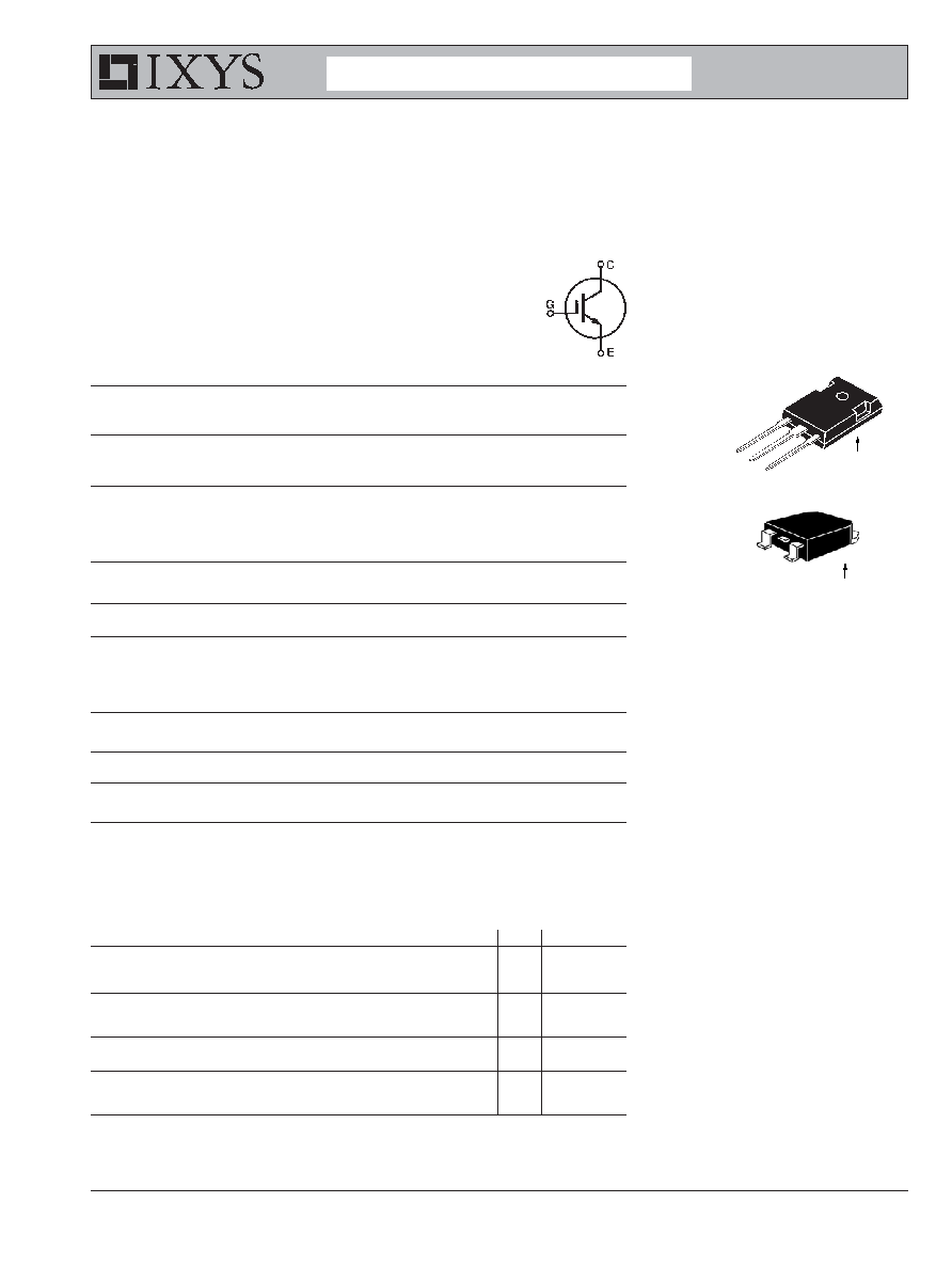
G = Gate,
C = Collector,
E = Emitter,
TAB = Collector
Features
High frequency IGBT
High current handling capability
MOS Gate turn-on
- drive simplicity
Applications
PFC circuits
Uninterruptible power supplies (UPS)
Switched-mode and resonant-mode
power supplies
AC motor speed control
DC servo and robot drives
DC choppers
Advantages
High power density
Very fast switching speeds for high
frequency applications
HiPerFAST
TM
IGBT
IXGH 50N90B2
IXGT 50N90B2
TO-268
(IXGT)
C (TAB)
C (TAB)
G
C
E
TO-247
(IXGH)
E
G
B2-Class High Speed IGBTs
Advance Technical Information
IXYS reserves the right to change limits, test conditions, and dimensions.
IXGH 50N90B2
IXGT 50N90B2
IXYS MOSFETs and IGBTs are covered by one or more
4,850,072
4,931,844
5,034,796
5,063,307
5,237,481
5,381,025
6,404,065B1
6,162,665
6,534,343
6,583,505
of the following U.S. patents:
4,835,592
4,881,106
5,017,508
5,049,961
5,187,117
5,486,715
6,306,728B1
6,259,123B1 6,306,728B1 6,683,344
Symbol
Test Conditions
Characteristic Values
(T
J
= 25
∞C, unless otherwise specified)
min.
typ.
max.
g
fs
I
C
= I
C110
A; V
CE
= 10 V,
25
40
S
Pulse test, t
300 µs, duty cycle 2 %
C
ies
2500
pF
C
oes
V
CE
= 25 V, V
GE
= 0 V, f = 1 MHz
180
pF
C
res
75
pF
Q
g
135
nC
Q
ge
I
C
= I
C110
A, V
GE
= 15 V, V
CE
= 0.5 V
CES
23
nC
Q
gc
50
nC
t
d(on)
20
ns
t
ri
28
ns
t
d(off)
350
500
ns
t
fi
200
ns
E
off
4.7
7.5 mJ
t
d(on)
20
ns
t
ri
28
ns
E
on
0.7
mJ
t
d(off)
400
ns
t
fi
420
ns
E
off
8.7
mJ
R
thJC
0.31 K/W
R
thCK
(TO-247)
0.25
K/W
Inductive load, T
J
= 25
∞∞
∞∞
∞
C
I
C
= I
C110
A, V
GE
= 15 V
V
CE
= 720 V, R
G
= R
off
= 5
Inductive load, T
J
= 125
∞∞
∞∞
∞
C
I
C
= I
C110
A, V
GE
= 15 V
V
CE
= 720 V, R
G
= R
off
= 5
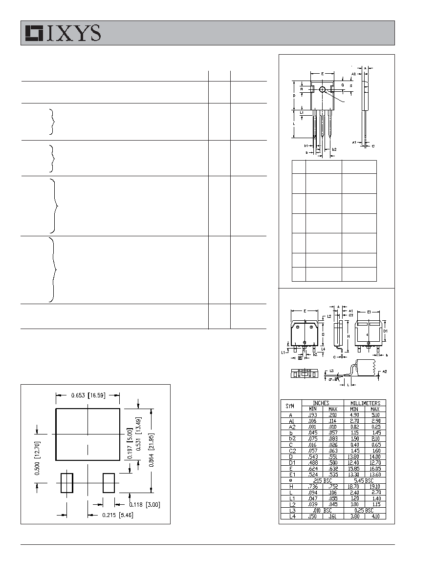
TO-247 AD Outline
Dim.
Millimeter
Inches
Min.
Max.
Min. Max.
A
4.7
5.3
.185
.209
A
1
2.2
2.54
.087
.102
A
2
2.2
2.6
.059
.098
b
1.0
1.4
.040
.055
b
1
1.65
2.13
.065
.084
b
2
2.87
3.12
.113
.123
C
.4
.8
.016
.031
D
20.80
21.46
.819
.845
E
15.75
16.26
.610
.640
e
5.20
5.72
0.205 0.225
L
19.81
20.32
.780
.800
L1
4.50
.177
P
3.55
3.65
.140
.144
Q
5.89
6.40
0.232 0.252
R
4.32
5.49
.170
.216
S
6.15 BSC
242 BSC
e
P
TO-268 Outline
Min. Recommended Footprint
(Dimensions in inches and mm)
© 2004 IXYS All rights reserved
IXGH 50N90B2
IXGT 50N90B2
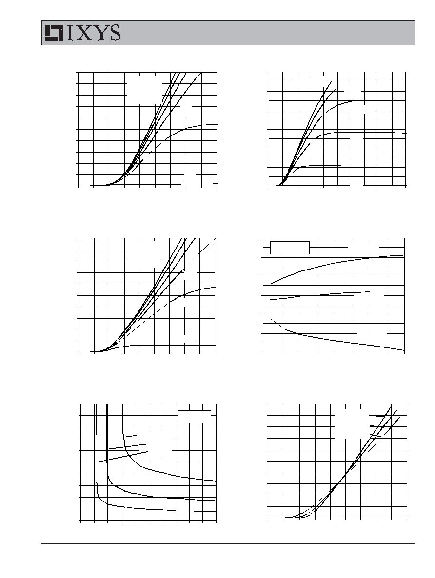
Fig. 2. Extended Output Characteristics
@ 25
∫
C
0
50
100
150
200
250
300
0
3
6
9
12
15
V
C E
- Volts
I
C
-
A
m
per
es
V
GE
= 15V
7V
9V
11V
13V
5V
Fig. 3. Output Characteristics
@ 125
∫
C
0
10
20
30
40
50
60
70
80
90
100
0
0.5
1
1.5
2
2.5
3
3.5
4
4.5
V
CE
- Volts
I
C
-
A
m
per
es
V
GE
= 15V
13V
11V
7V
5V
9V
Fig. 1. Output Characteristics
@ 25
∫
C
0
10
20
30
40
50
60
70
80
90
100
0
0.5
1
1.5
2
2.5
3
3.5
4
4.5
V
C E
- Volts
I
C
-
A
m
per
es
V
GE
=15V
13V
11V
9V
5V
7V
Fig. 4. Dependence of V
CE(sat)
on
Tem perature
0.7
0.8
0.9
1.0
1.1
1.2
1.3
-50
-25
0
25
50
75
100
125
150
T
J
- Degrees Centigrade
V
C E
(
s
a
t
)
- N
o
rm
a
l
i
z
e
d
I
C
= 50A
I
C
= 25A
V
GE
= 15V
I
C
= 100A
Fig. 5. Collector-to-Em itter Voltage
vs. Gate-to-Em itter voltage
1.5
2.0
2.5
3.0
3.5
4.0
4.5
5.0
5.5
6.0
6.5
5
6
7
8
9
10
11
12
13
14
15
V
G E
- Volts
V
C E
- V
o
l
t
s
T
J
= 25
∫
C
I
C
= 100A
50A
25A
Fig. 6. Input Adm ittance
0
25
50
75
100
125
150
175
200
225
250
3
4
5
6
7
8
9
10
11
12
V
G E
- Volts
I
C
-
A
m
per
es
T
J
= -40
∫
C
25
∫
C
125
∫
C
IXYS reserves the right to change limits, test conditions, and dimensions.
IXGH 50N90B2
IXGT 50N90B2
IXYS MOSFETs and IGBTs are covered by one or more
4,850,072
4,931,844
5,034,796
5,063,307
5,237,481
5,381,025
6,404,065B1
6,162,665
6,534,343
6,583,505
of the following U.S. patents:
4,835,592
4,881,106
5,017,508
5,049,961
5,187,117
5,486,715
6,306,728B1
6,259,123B1 6,306,728B1 6,683,344
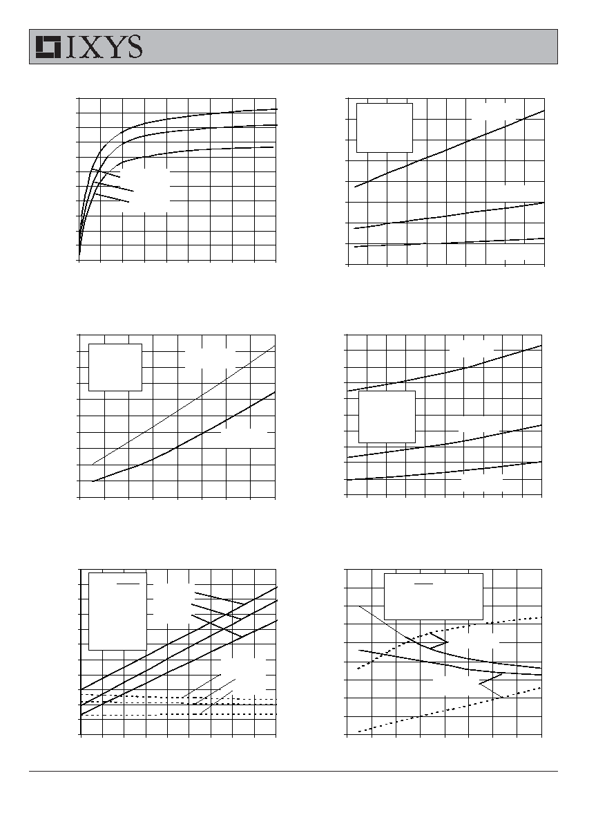
Fig. 7. Transconductance
0
5
10
15
20
25
30
35
40
45
50
55
0
25
50
75
100 125 150
175 200 225
I
C
- Amperes
g
f s
-
S
i
em
ens
T
J
= -40
∫
C
25
∫
C
125
∫
C
Fig. 8. Dependence of Turn-off
Energy Loss on R
G
0
5
10
15
20
25
30
35
40
0
30
60
90
120
150
R
G
- Ohms
E
o
f f
-
m
i
l
liJ
o
u
les
I
C
= 25A
T
J
= 125
∫
C
V
GE
= 15V
V
CE
= 720V
I
C
= 50A
I
C
= 100A
Fig. 9. Dependence of Turn-Off
Energy Loss on I
C
0
2
4
6
8
10
12
14
16
18
20
20
30
40
50
60
70
80
90
100
I
C
- Amperes
E
o f
f
-
M
i
l
liJ
oul
es
R
G
= 5
V
GE
= 15V
V
CE
= 720V
T
J
= 125
∫
C
T
J
= 25
∫
C
Fig. 10. Dependence of Turn-off
Energy Loss on Tem perature
0
2
4
6
8
10
12
14
16
18
20
25
35
45
55
65
75
85
95 105 115 125
T
J
- Degrees Centigrade
E
o f
f
-
m
ill
iJ
oules
I
C
= 100A
R
G
= 5
V
GE
= 15V
V
CE
= 720V
I
C
= 50A
I
C
= 25A
Fig. 11. Dependence of Turn-off
Sw itching Tim e on R
G
200
300
400
500
600
700
800
900
1000
1100
1200
1300
5
10
15
20
25
30
35
40
45
50
R
G
- Ohms
S
w
it
c
h
ing T
i
m
e
-
nanos
ec
onds
t
d(off)
t
fi
- - - - - -
T
J
= 125∫C
V
GE
= 15V
V
CE
= 720V
I
C
= 100A
50A
25A
I
C
= 25A
50A
100A
Fig. 12. Dependence of Turn-off
Sw itching Tim e
on I
C
150
200
250
300
350
400
450
500
550
600
20
30
40
50
60
70
80
90
100
I
C
- Amperes
S
w
i
t
c
h
ing T
i
m
e
-
nanos
ec
onds
t
d(off)
t
fi
- - - - -
R
G
= 5, V
GE
= 15V
V
CE
= 720V
T
J
= 125
∫
C
T
J
= 25
∫
C
© 2004 IXYS All rights reserved
IXGH 50N90B2
IXGT 50N90B2
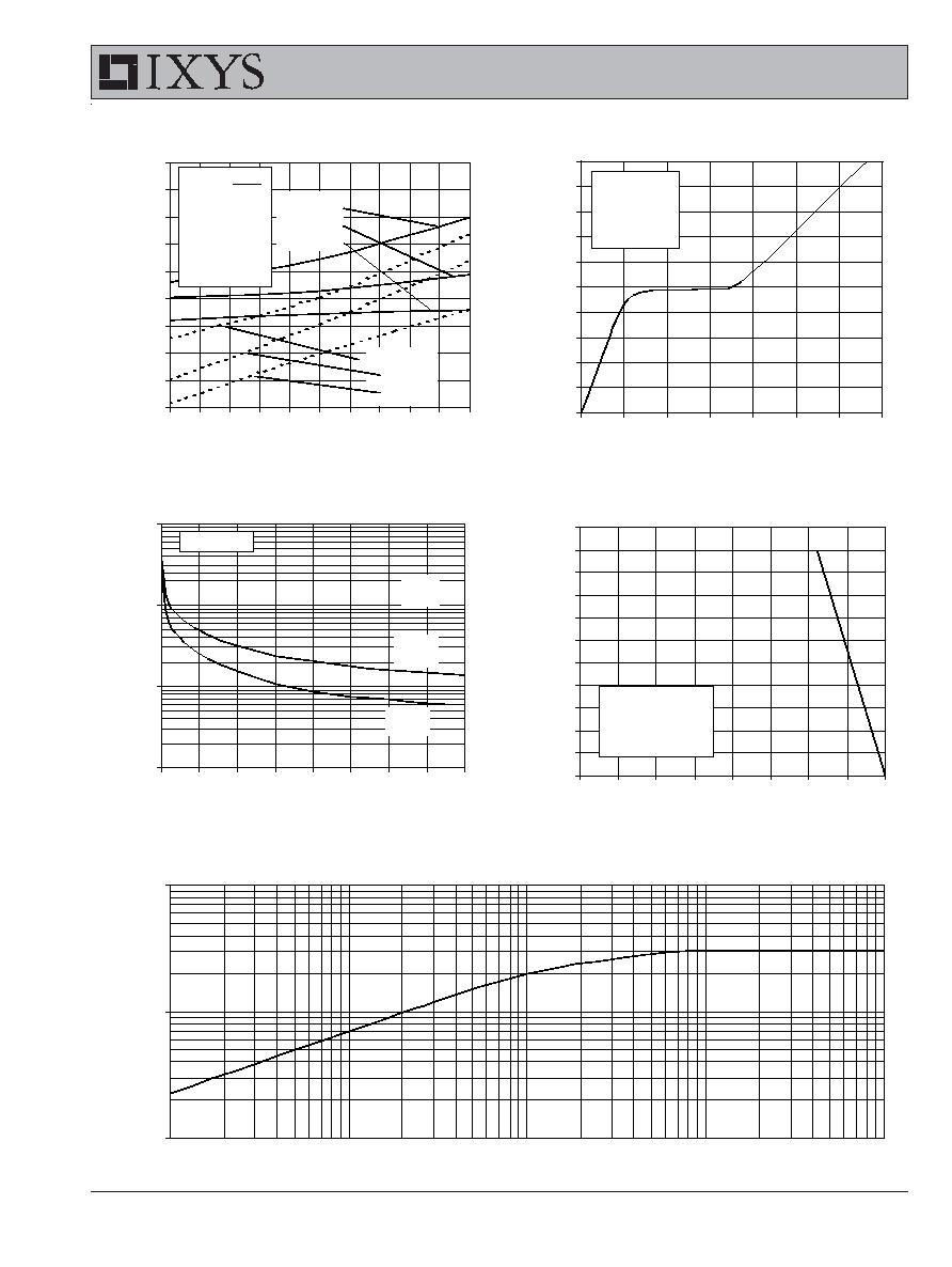
Fig. 14. Gate Charge
0
1.5
3
4.5
6
7.5
9
10.5
12
13.5
15
0
20
40
60
80
100
120
140
Q
G
- nanoCoulombs
V
G E
- V
o
l
t
s
V
CE
= 450V
I
C
= 50A
I
G
= 10mA
Fig. 15. Capacitance
10
100
1000
10000
0
5
10
15
20
25
30
35
40
V
C E
- Volts
C
a
pa
c
i
t
a
nc
e
-
p F
C
ies
C
oes
C
res
f = 1 MHz
Fig. 13. Dependence of Turn-off
Sw itching Tim e on Tem perature
150
200
250
300
350
400
450
500
550
600
25
35
45
55
65
75
85
95
105 115 125
T
J
- Degrees Centigrade
S
w
i
t
c
h
ing
T
i
m
e
-
na
nos
e
c
on
ds
t
d(off)
t
fi
- - - - - -
R
G
=
5
V
GE
=
15V
V
CE
=
720V
I
C
= 100A
50A
25A
I
C
= 25A
50A
100A
Fig. 16. Reverse-Bias Safe
Operating Area
0
10
20
30
40
50
60
70
80
90
100
110
100
200
300
400
500
600
700
800
900
V
C E
- Volts
I
C
- A
m
p
e
r
e
s
T
J
= 125
∫
C
R
G
= 10
dV/dT < 10V/ns
Fig. 17. Maxim um Transient Thermal Resistance
0.01
0.1
1
0.1
1
10
100
1000
Pulse Width - milliseconds
R
(
t
h
)
J
C
-
∫
C
/ W