© 2004 IXYS All rights reserved
Symbol
Test Conditions
Characteristic Values
(T
J
= 25
∞C, unless otherwise specified)
Min.
Typ. Max.
V
GE(th)
I
C
= 250
µA, V
CE
= V
GE
3.0
5.0
V
I
CES
V
CE
= V
CES
T
J
= 25
∞C
650
µA
V
GE
= 0 V
T
J
= 125
∞C
5
mA
I
GES
V
CE
= 0 V, V
GE
=
±20 V
±100
nA
V
CE(sat)
I
C
= 40 A, V
GE
= 15 V
T
J
= 25
∞C
2.1
2.5
V
Note 1
T
J
= 125
∞C
1.8
V
HiPerFAST
TM
IGBT with Diode
Symbol
Test Conditions
Maximum Ratings
V
CES
T
J
= 25
∞C to 150∞C
600
V
V
CGR
T
J
= 25
∞C to 150∞C; R
GE
= 1 M
600
V
V
GES
Continuous
±20
V
V
GEM
Transient
±30
V
I
C25
T
C
= 25
∞C (limited by leads)
75
A
I
C110
T
C
= 110
∞C
50
A
I
F110
T
C
= 110
∞C
48
A
I
CM
T
C
= 25
∞C, 1 ms
300
A
SSOA
V
GE
= 15 V, T
VJ
= 125
∞C, R
G
= 10
I
CM
= 100
A
(RBSOA)
Clamped inductive load @ V
CE
600 V
P
C
T
C
= 25
∞C
480
W
T
J
-55 ... +150
∞C
T
JM
150
∞C
T
stg
-55 ... +150
∞C
M
d
Mounting torque, TO-264
1.13/10 Nm/lb.in.
Weight
TO-264
10
g
PLUS247
6
g
Maximum lead temperature for soldering
300
∞C
1.6 mm (0.062 in.) from case for 10 s
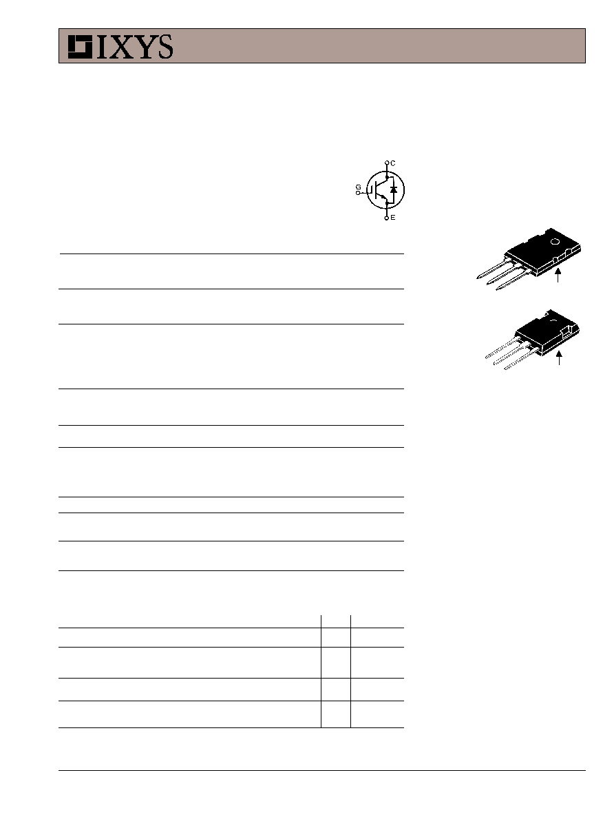
G = Gate
C = Collector
E = Emitter
Tab = Collector
Features
∑
Very high frequency IGBT and
anti-parallel FRED in one package
∑
Square RBSOA
∑
High current handling capability
∑
MOS Gate turn-on for drive simplicity
∑
Fast Recovery Epitaxial Diode (FRED)
with soft recovery and low I
RM
Applications
∑
Switch-mode and resonant-mode
power supplies
∑
Uninterruptible power supplies (UPS)
∑
DC choppers
∑
AC motor speed control
∑
DC servo and robot drives
Advantages
∑
Space savings (two devices in one
package)
∑
Easy to mount with 1 screw
G
C
E
TO-264 AA
(IXGK)
DS99148A(05/04)
PLUS247
(IXGX)
V
CES
= 600 V
I
C25
= 75 A
V
CE(sat)
= 2.5 V
t
fi(typ)
= 48 ns
(TAB)
(TAB)
IXGK50N60C2D1
IXGX 50N60C2D1
C2-Class High Speed IGBTs
Preliminary Data Sheet
G
E
C

IXYS reserves the right to change limits, test conditions, and dimensions.
IXGK 50N60C2D1
IXGX 50N60C2D1
Symbol
Test Conditions
Characteristic Values
(T
J
= 25
∞C, unless otherwise specified)
Min. Typ. Max.
g
fs
I
C
= 40 A; V
CE
= 10 V,
40
51
S
Note 1
C
ies
3700
pF
C
oes
V
CE
= 25 V, V
GE
= 0 V, f = 1 MHz
290
pF
C
res
50
pF
Q
g
138
nC
Q
ge
I
C
= 40 A, V
GE
= 15 V, V
CE
= 0.5 V
CES
25
nC
Q
gc
40
nC
t
d(on)
18
ns
t
ri
25
ns
t
d(off)
115 150
ns
t
fi
48
ns
E
off
0.38
0.7 mJ
t
d(on)
18
ns
t
ri
25
ns
E
on
1.4
mJ
t
d(off)
170
ns
t
fi
60
ns
E
off
0.74
mJ
R
thJC
0.31 K/W
R
thCK
0.15
K/W
Inductive load, T
J
= 25
∞∞
∞∞
∞C
I
C
= 40 A, V
GE
= 15 V
V
CE
= 480 V, R
G
= R
off
= 2.0
Inductive load, T
J
= 125
∞∞
∞∞
∞C
I
C
= 40 A, V
GE
= 15 V
V
CE
= 480 V, R
G
= R
off
= 2.0
PLUS247 Outline
Dim.
Millimeter
Inches
Min.
Max.
Min. Max.
A
4.83
5.21
.190
.205
A
1
2.29
2.54
.090
.100
A
2
1.91
2.16
.075
.085
b
1.14
1.40
.045
.055
b
1
1.91
2.13
.075
.084
b
2
2.92
3.12
.115
.123
C
0.61
0.80
.024
.031
D
20.80
21.34
.819
.840
E
15.75
16.13
.620
.635
e
5.45 BSC
.215 BSC
L
19.81
20.32
.780
.800
L1
3.81
4.32
.150
.170
Q
5.59
6.20
.220 0.244
R
4.32
4.83
.170
.190
Terminals:
1 - Gate
2 - Drain (Collector)
3 - Source (Emitter)
4 - Drain (Collector)
TO-264 AA Outline
Millimeter
Inches
Min.
Max.
Min.
Max.
A
4.82
5.13
.190
.202
A1
2.54
2.89
.100
.114
A2
2.00
2.10
.079
.083
b
1.12
1.42
.044
.056
b1
2.39
2.69
.094
.106
b2
2.90
3.09
.114
.122
c
0.53
0.83
.021
.033
D
25.91
26.16
1.020
1.030
E
19.81
19.96
.780
.786
e
5.46 BSC
.215 BSC
J
0.00
0.25
.000
.010
K
0.00
0.25
.000
.010
L
20.32
20.83
.800
.820
L1
2.29
2.59
.090
.102
P
3.17
3.66
.125
.144
Q
6.07
6.27
.239
.247
Q1
8.38
8.69
.330
.342
R
3.81
4.32
.150
.170
R1
1.78
2.29
.070
.090
S
6.04
6.30
.238
.248
T
1.57
1.83
.062
.072
Dim.
Reverse Diode (FRED)
Characteristic Values
(T
J
= 25∞C, unless otherwise specified)
Symbol
Test Conditions
min.
typ.
max.
V
F
I
F
= 60 A, V
GE
= 0 V,
2.1
V
Note 1
T
J
= 150
∞C
1.4
I
RM
I
F
= 60 A, V
GE
= 0 V, -di
F
/dt = 100 A/
µ T
J
= 100
∞C
8.3
A
V
R
= 100 V
t
rr
I
F
= 1 A; -di/dt = 200 A/ms; V
R
= 30 V
35
ns
R
thJC
0.65 K/W
Note 1: Pulse test, t
300 µs, duty cycle 2 %
IXYS MOSFETs and IGBTs are covered by one or more
of the following U.S. patents:
4,835,592 4,881,106 5,017,508 5,049,961 5,187,117 5,486,715 6,306,728B1 6,259,123B1 6,306,728B1
4,850,072 4,931,844 5,034,796 5,063,307 5,237,481 5,381,025 6,404,065B1 6,162,665 6,534,343 6,583,505
© 2004 IXYS All rights reserved
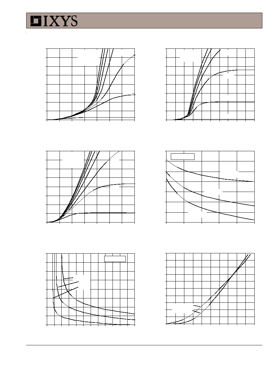
Fig. 2. Extended Output Characteristics
@ 25 deg. C
0
40
80
120
160
200
240
280
320
0
1
2
3
4
5
6
7
8
9
10
V
C E
- Volts
I
C
-
A
m
per
es
V
GE
= 15V
13V
5V
7V
9V
11V
Fig. 3. Output Characteristics
@ 125 Deg. C
0
10
20
30
40
50
60
70
80
0.5
1
1.5
2
2.5
3
3.5
4
V
CE
- Volts
I
C
-
A
m
per
es
V
GE
= 15V
13V
11V
6V
5V
7V
9V
Fig. 1. Output Characteristics
@ 25 Deg. C
0
10
20
30
40
50
60
70
80
0.5
1
1.5
2
2.5
3
3.5
4
V
C E
- Volts
I
C
-
A
m
per
es
V
GE
= 15V
13V
11V
7V
5V
6V
9V
Fig. 4. Dependence of V
CE(sat)
on
Tem perature
0.5
0.6
0.7
0.8
0.9
1.0
1.1
1.2
25
50
75
100
125
150
T
J
- Degrees Centigrade
V
C E
( s
a
t
)
- N
o
rm
a
l
i
z
e
d
I
C
= 40A
I
C
= 20A
V
GE
= 15V
I
C
= 80A
Fig. 5. Collector-to-Em itter Voltage
vs. Gate-to-Em itter voltage
2.4
2.7
3
3.3
3.6
3.9
4.2
4.5
4.8
5
6
7
8
9
10 11 12 13 14 15 16 17
V
G E
- Volts
V
C E
-
V
o
l
t
s
T
J
= 25∫C
I
C
= 80A
40A
20A
Fig. 6. Input Adm ittance
0
20
40
60
80
100
120
140
160
180
200
4
4.5
5
5.5
6
6.5
7
7.5
8
8.5
9
V
G E
- Volts
I
C
-
A
m
per
es
T
J
= 125∫C
25∫C
IXGK 50N60C2D1
IXGX 50N60C2D1
IXYS reserves the right to change limits, test conditions, and dimensions.
IXGK 50N60C2D1
IXGX 50N60C2D1
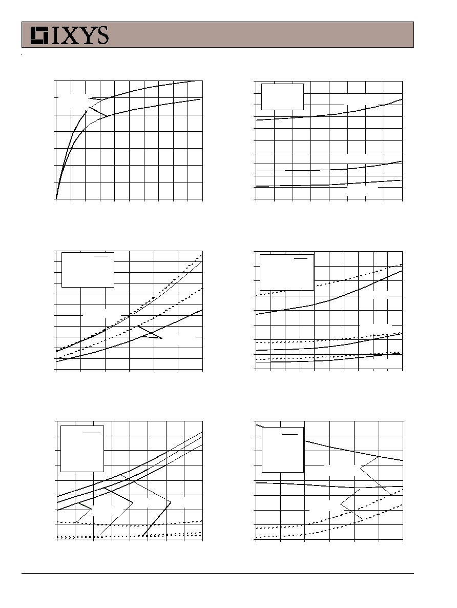
Fig. 7. Transconductance
0
10
20
30
40
50
60
70
0
20
40
60
80
100 120 140 160 180 200
I
C
- Amperes
g
f s
-
S
i
em
ens
T
J
= 25∫C
125∫C
Fig. 8. Dependence of Turn-Off
Energy on R
G
0
0.3
0.6
0.9
1.2
1.5
1.8
2.1
2.4
2.7
3
2
4
6
8
10
12
14
16
18
R
G
- Ohms
E
o
f f
-
m
illiJ
o
u
l
e
s
I
C
= 20A
T
J
= 125∫C
V
GE
= 15V
V
CE
= 480V
I
C
= 40A
I
C
= 80A
Fig. 9. Dependence of Turn-Off
Energy
on I
c
0
0.2
0.4
0.6
0.8
1
1.2
1.4
1.6
1.8
2
2.2
20
30
40
50
60
70
80
I
C
- Amperes
E
o f
f
-
M
illiJ
o
u
l
e
s
R
G
= 2
R
G
= 10 - - - -
V
GE
= 15V
V
CE
= 480V
T
J
= 125∫C
T
J
= 25∫C
Fig. 10. Dependence of Turn-Off
Energy on Tem perature
0
0.3
0.6
0.9
1.2
1.5
1.8
2.1
2.4
25
35
45
55
65
75
85
95
105 115 125
T
J
- Degrees Centigrade
E
o f
f
-
m
illiJ
o
u
l
e
s
I
C
= 80A
R
G
= 2
R
G
= 10 - - - -
V
GE
= 15V
V
CE
= 480V
I
C
= 40A
I
C
= 20A
Fig. 11. Dependence of Turn-Off
Sw itching Tim e on R
G
50
100
150
200
250
300
350
400
450
2
4
6
8
10
12
14
16
18
R
G
- Ohms
S
w
i
t
c
h
i
ng T
i
m
e
-
nanos
ec
onds
I
C
= 20A
t
d(off)
t
fi
-
- - - - -
T
J
= 125∫C
V
GE
= 15V
V
CE
= 480V
I
C
= 40A
I
C
= 80A
Fig. 12. Dependence of Turn-Off
Sw itching Tim e
on I
c
40
60
80
100
120
140
160
180
200
20
30
40
50
60
70
80
I
C
- Amperes
S
w
i
t
c
h
i
ng T
i
m
e
-
nano
s
e
c
onds
t
d(off)
t
fi
- - - - - -
R
G
= 2
V
GE
= 15V
V
CE
= 480V
T
J
= 125∫C
T
J
= 25∫C

© 2004 IXYS All rights reserved
Fig. 15. Gate Charge
0
2
4
6
8
10
12
14
16
0
30
60
90
120
150
Q
G
- nanoCoulombs
V
G E
- V
o
l
t
s
V
CE
= 300V
I
C
= 40A
I
G
= 10mA
Fig. 16. Capacitance
10
100
1000
10000
0
5
10
15
20
25
30
35
40
V
C E
- Volts
Ca
p
a
c
i
t
a
nc
e -
pi
c
o
F
a
r
r
a
d
s
C
ies
C
oes
C
res
f = 1 MHz
Fig. 13. Dependence of Turn-Off
Sw itching Tim e on Tem perature
20
40
60
80
100
120
140
160
180
200
25
35
45
55
65
75
85
95
105 115 125
T
J
- Degrees Centigrade
S
w
it
c
h
i
n
g T
i
m
e
-
na
no
s
e
c
o
n
d
s
I
C
= 80A
t
d(off)
t
fi
-
- - - - -
R
G
= 2
V
GE
= 15V
V
CE
= 480V
I
C
= 20A
I
C
= 40A
I
C
= 20A
Fig. 16. Maxim um Transient Therm al Resistance
0.00
0.05
0.10
0.15
0.20
0.25
0.30
0.35
1
10
100
1000
Pulse Width - milliseconds
R
( t
h
) J
C
-
∫C
/
W
Fig. 14. Reverse-Bias
Safe Operating Area
0
10
20
30
40
50
60
70
80
90
100
110
100
200
300
400
500
600
V
C E
- Volts
I
C
- A
m
p
e
re
s
T
J
= 125
∫
C
R
G
= 10
dV/dT < 10V/ns
IXGK 50N60C2D1
IXGX 50N60C2D1

IXYS reserves the right to change limits, test conditions, and dimensions.
IXGK 50N60C2D1
IXGX 50N60C2D1
200
600
1000
0
400
800
80
90
100
110
120
130
140
0.00001
0.0001
0.001
0.01
0.1
1
0.0001
0.001
0.01
0.1
1
0
40
80
120
160
0.0
0.5
1.0
1.5
2.0
K
f
T
VJ
∞C
-di
F
/dt
t
s
K/W
0
200
400
600
800 1000
0
5
10
15
20
0.0
0.4
0.8
1.2
1.6
V
FR
di
F
/dt
V
200
600
1000
0
400
800
0
20
40
60
80
100
1000
0
1000
2000
3000
4000
0
1
2
0
20
40
60
80
100
120
140
160
I
RM
Q
r
I
F
A
V
F
-di
F
/dt
-di
F
/dt
A/
µs
A
V
nC
A/
µs
A/
µs
t
rr
ns
t
fr
A/
µs
µs
DSEP 60-06A
Z
thJC
I
F
=120A
I
F
= 60A
I
F
= 30A
T
VJ
= 100∞C
V
R
= 300V
T
VJ
= 100∞C
I
F
= 60A
Fig. 19. Peak reverse current I
RM
versus -di
F
/dt
Fig. 18. Reverse recovery charge Q
r
versus -di
F
/dt
Fig. 17. Forward current I
F
versus V
F
T
VJ
= 100∞C
V
R
= 300V
T
VJ
= 100∞C
V
R
= 300V
I
F
=120A
I
F
= 60A
I
F
= 30A
Q
r
I
RM
Fig. 20. Dynamic parameters Q
r
, I
RM
versus T
VJ
Fig. 21. Recovery time t
rr
versus -di
F
/dt
Fig. 22. Peak forward voltage V
FR
and
t
fr
versus di
F
/dt
I
F
=120A
I
F
= 60A
I
F
= 30A
t
fr
V
FR
Fig. 23. Transient thermal resistance junction to case
Constants for Z
thJC
calculation:
i
R
thi
(K/W)
t
i
(s)
1
0.324
0.0052
2
0.125
0.0003
3
0.201
0.0385
T
VJ
= 25∞C
T
VJ
=150∞C
T
VJ
=100∞C
Note: Fig. 2 through Fig. 6 show typical
values