© 2001 IXYS All rights reserved
98803 (01/01)
V
CES
= 600 V
I
C25
=
75 A
V
CE(sat)
=
2.5
V
t
fi(typ)
=
75
ns
HiPerFAST
TM
IGBT
ISOPLUS247
TM
(Electrically Isolated Backside)
ISOPLUS 247
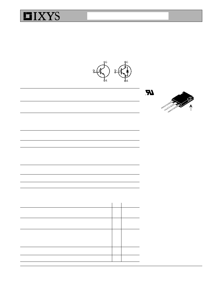
G = Gate,
C = Collector
E = Emitter
* Patent pending
E153432
Symbol
Test Conditions
Maximum Ratings
V
CES
T
J
= 25∞C to 150∞C
600
V
V
CGR
T
J
= 25∞C to 150∞C; R
GE
= 1 MW
600
V
V
GES
Continuous
±20
V
V
GEM
Transient
±30
V
I
C25
T
C
= 25∞C
75
A
I
C110
T
C
= 110∞C
35
A
I
CM
T
C
= 25∞C, 1 ms
150
A
SSOA
V
GE
= 15 V, T
VJ
= 125∞C, R
G
= 10 W
I
CM
= 80
A
(RBSOA)
Clamped inductive load
@ 0.8 V
CES
P
C
T
C
= 25∞C
200
W
T
J
-55 ... +150
∞C
T
JM
150
∞C
T
stg
-55 ... +150
∞C
Maximum lead temperature for soldering
300
∞C
1.6 mm (0.062 in.) from case for 10 s
M
d
Mounting torque (M3)
1.13/10Nm/lb.in.
Weight
5
g
G
C
E
Isolated Backside*
Symbol
Test Conditions
Characteristic Values
(T
J
= 25∞C, unless otherwise specified)
Min. Typ. Max.
BV
CES
I
C
= 250 mA, V
GE
= 0 V
40N60C
600
V
I
C
= 750 mA
40N60CD1
600
V
GE(th)
I
C
= 250 mA, V
CE
= V
GE
40N60C
2.5
5.0
V
I
C
= 500 mA
40N60CD1
2.5
5.0
V
I
CES
V
CE
=
0.8 ∑ V
CES
T
J
= 25∞C
40N60C
200
mA
V
GE
= 0 V; note 1
T
J
= 25∞C
40N60CD1
650
mA
T
J
= 125∞C
40N60C
1 mA
T
J
= 125∞C
40N60CD1
3 mA
I
GES
V
CE
= 0 V, V
GE
= ±20 V
±100 nA
V
CE(sat)
I
C
=
I
T
,
V
GE
= 15 V
2.5
V
Features
l
DCB Isolated mounting tab
l
Meets TO-247AD package Outline
l
High current handling capability
l
Latest generation HDMOS
TM
process
l
MOS Gate turn-on
- drive simplicity
Applications
l
Uninterruptible power supplies (UPS)
l
Switched-mode and resonant-mode
power supplies
l
AC motor speed control
l
DC servo and robot drives
l
DC choppers
Advantages
l
Easy assembly
l
High power density
l
Very fast switching speeds for high
frequency applications
IXGR 40N60C
IXGR 40N60CD1
(D1)
Advanced Technical Information

IXYS MOSFETS and IGBTs are covered by one or more of the following U.S. patents:
4,835,592
4,881,106
5,017,508
5,049,961
5,187,117
5,486,715
4,850,072
4,931,844
5,034,796
5,063,307
5,237,481
5,381,025
IXYS reserves the right to change limits, test conditions, and dimensions.
IXGR 40N60C
IXGR 40N60CD1
Symbol
Test Conditions
Characteristic Values
(T
J
= 25
∞
C, unless otherwise specified)
min.
typ.
max.
g
fs
I
C
= I
T
; V
CE
= 10 V,
30
40
S
Pulse test, t
£
300
m
s, duty cycle
£
2 %
C
ies
3300
pF
40N60C
310
pF
C
oes
V
CE
= 25 V, V
GE
= 0 V, f = 1 MHz
40N60CD1
370
pF
C
res
65
pF
Q
g
116
nC
Q
ge
I
C
= I
T
, V
GE
= 15 V, V
CE
= 0.5 V
CES
23
nC
Q
gc
55
nC
t
d(on)
25
n s
t
ri
30
n s
t
d(off)
100
150
ns
t
fi
75
150
ns
E
off
0.85
1.70
mJ
t
d(on)
25
n s
t
ri
35
ns
E
on
40N60C
0.4
mJ
t
d(off)
40N60CD1
1.2
mJ
t
fi
150
ns
105
ns
E
off
1.2
mJ
R
thJC
0.6 K/W
R
thCK
0.15
K/W
Inductive load, T
J
= 25
∞
C
I
C
= I
T
, V
GE
= 15 V
V
CE
= 0.8 ∑ V
CES
, R
G
= R
off
= 4.7
W
Remarks: Switching times may increase
for V
CE
(Clamp) > 0.8 ∑ V
CES
, higher T
J
or
increased R
G
Inductive load, T
J
= 125
∞
C
I
C
= I
T
, V
GE
= 15 V
V
CE
= 0.8 ∑ V
CES
, R
G
= R
off
= 4.7
W
Remarks: Switching times may increase for
V
CE
(Clamp) > 0.8 ∑ V
CES
, higher T
J
or
increased R
G
ISOPLUS 247 OUTLINE
Dim.
Millimeter
Inches
Min.
Max.
Min. Max.
A
4.83
5.21
.190 .205
A
1
2.29
2.54
.090 .100
A
2
1.91
2.16
.075 .085
b
1.14
1.40
.045 .055
b
1
1.91
2.13
.075 .084
b
2
2.92
3.12
.115 .123
C
0.61
0.80
.024 .031
D
20.80 21.34
.819 .840
E
15.75 16.13
.620 .635
e 5.45 BSC
.215 BSC
L
19.81 20.32
.780 .800
L1
3.81
4.32
.150 .170
Q
5.59
6.20
.220 .244
R
4.32
4.83
.170 .190
1 Gate, 2 Drain (Collector)
3 Source (Emitter)
4 no connection
Reverse Diode (FRED) (IXGH40N60CD1 only)
Characteristic Values
(T
J
= 25∞C, unless otherwise specified)
Symbol
Test Conditions
min.
typ. max.
V
F
I
F
=
I
T
, V
GE
= 0 V,
T
J
= 150∞C
1.3
V
Note 1
T
J
= 25∞C
1.8
V
I
RM
I
F
=
I
T
, V
GE
= 0 V, V
R
= 100 V
T
J
= 100∞C
7.5
A
-di
F
/dt = 100 A/ms
t
rr
I
F
= 1 A; -di/dt = 100 A/ms; V
R
= 30 V
3.5
ns
R
thJC
0.90 K/W
Note:
1. Pulse test,
t
p
£ 300 ms, duty cycle:d £ 2 %
2. I
T
= 40A