© 2004 IXYS All rights reserved
Features
DCB Isolated mounting tab
Meets TO-247AD package Outline
High current handling capability
Latest generation HDMOS
TM
process
MOS Gate turn-on
- drive simplicity
Applications
Uninterruptible power supplies (UPS)
Switched-mode and resonant-mode
power supplies
AC motor speed control
DC servo and robot drives
DC choppers
Advantages
Easy assembly
High power density
Very fast switching speeds for high
frequency applications
ISOLATED TAB
DS99052B(09/03)
Symbol
Test Conditions
Maximum Ratings
V
CES
T
J
= 25
∞
C to 150
∞
C
600
V
V
CGR
T
J
= 25
∞
C to 150
∞
C; R
GE
= 1 M
600
V
V
GES
Continuous
±
20
V
V
GEM
Transient
±
30
V
I
C25
T
C
= 25
∞
C
56
A
I
C110
T
C
= 110
∞
C
26
A
I
D110
T
C
= 110
∞
C (40N60C2D1)
27
A
I
CM
T
C
= 25
∞
C, 1 ms
200
A
SSOA
V
GE
= 15 V, T
VJ
= 125
∞
C, R
G
= 10
I
CM
= 80
A
(RBSOA)
Clamped inductive load @ V
CE
600 V
P
C
T
C
= 25
∞
C
170
W
T
J
-55 ... +150
∞
C
T
JM
150
∞
C
T
stg
-55 ... +150
∞
C
Maximum Lead temperature for soldering
300
∞
C
1.6 mm (0.062 in.) from case for 10 s
V
ISOL
50/60 Hz RMS, t = 1m
2500
V
Weight
4
g
HiPerFAST
TM
IGBT
ISOPLUS247
TM
C2-Class High Speed IGBTs
V
CES
= 600 V
I
C25
= 56 A
V
CE(SAT)
= 2.7 V
t
fi(typ)
= 32 ns
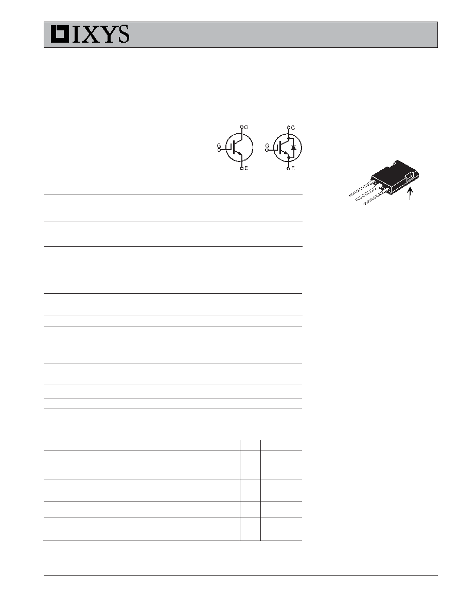
G = Gate
C = Collector
E = Emitter
IXGR 40N60C2
IXGR 40N60C2D1
(Electrically Isolated Back Surface)
IXGR_C2D1
IXGR_C2
ISOPLUS 247
TM
(IXGR)
G
C
E
Symbol
Test Conditions
Characteristic Values
(T
J
= 25
∞
C, unless otherwise specified)
min.
typ.
max.
BV
CES
I
C
= 250
A, V
GE
= 0 V
600
V
V
GE(th)
I
C
= 250
A, V
CE
= V
GE
3.0
5.0
V
I
CES
V
CE
= V
CES
40N60C2
50
A
V
GE
= 0 V
40N60C2/D1
100
A
I
GES
V
CE
= 0 V, V
GE
=
±
20 V
±
100
nA
V
CE(sat)
I
C
= 30 A, V
GE
= 15 V
T
J
= 25
∞
C
2.2
2.7
V
T
J
= 125
∞
C
2.0
V

IXYS reserves the right to change limits, test conditions, and dimensions.
IXYS MOSFETs and IGBTs are covered by one or more
of the following U.S. patents:
4,835,592 4,881,106 5,017,508 5,049,961 5,187,117 5,486,715 6,306,728B1 6,259,123B1 6,306,728B1
4,850,072 4,931,844 5,034,796 5,063,307 5,237,481 5,381,025 6,404,065B1 6,162,665 6,534,343
Symbol
Test Conditions
Characteristic Values
(T
J
= 25
∞
C, unless otherwise specified)
min.
typ.
max.
g
fs
I
C
= 30 A; V
CE
= 10 V,
20
36
S
Pulse test, t
300
s, duty cycle
2 %
C
ies
2500
pF
C
oes
V
CE
= 25 V, V
GE
= 0 V, f = 1 MHz 40N60C2
180
pF
40N60C2D1
220
pF
C
res
54
pF
Q
g
95
nC
Q
ge
I
C
= 30 A, V
GE
= 15 V, V
CE
= 0.5 V
CES
14
nC
Q
gc
36
nC
t
d(on)
18
ns
t
ri
20
ns
t
d(off)
90
140
ns
t
fi
32
90
ns
E
off
0.20
0.37 mJ
t
d(on)
18
ns
t
ri
20
ns
E
on
0.6
mJ
t
d(off)
130
ns
t
fi
80
240
ns
E
off
0.50
mJ
R
thJ-DCB
(Note 1)
0.26
0.42 K/W
R
thJC
(Note 2)
0.74 K/W
R
thCS
0.15
K/W
Reverse Diode (FRED) (D1 Version Only)
Characteristic Values
(T
J
= 25
∞
C, unless otherwise specified)
Symbol
Test Conditions
min.
typ.
max.
V
F
I
F
= 30 A, V
GE
= 0 V, Pulse test T
J
=150
∞
C
1.6
V
t
300
s, duty cycle d
2 % T
J
= 25
∞
C
2.5
V
I
RM
I
F
= 30 A, V
GE
= 0 V, -di
F
/dt =100 A/
s, T
J
= 100
∞
C
4
A
t
rr
V
R
= 100 V
100
ns
t
rr
I
F
= 1 A; -di/dt = 100 A/
s; V
R
= 30 V
25
ns
R
thJC
1.5 K/W
R
thCS
0.15
K/W
Inductive load, T
J
= 25
∞∞
∞∞
∞
C
I
C
= 30 A, V
GE
= 15 V
V
CE
= 400 V, R
G
= R
off
= 3
Inductive load, T
J
= 125
∞∞
∞∞
∞
C
I
C
= 30 A, V
GE
= 15 V
V
CE
= 400 V, R
G
= R
off
= 3
ISOPLUS 247 Outline
Notes:
1. R
thJ-DCB
is the thermal resistance junction-to-internal side of DCB substrate
2. R
thJC
is the thermal resistance junction-to-external side of DCB substrate
IXGR 40N60C2
IXGR 40N60C2D1
© 2004 IXYS All rights reserved
IXGR 40N60C2
IXGR 40N60C2D1
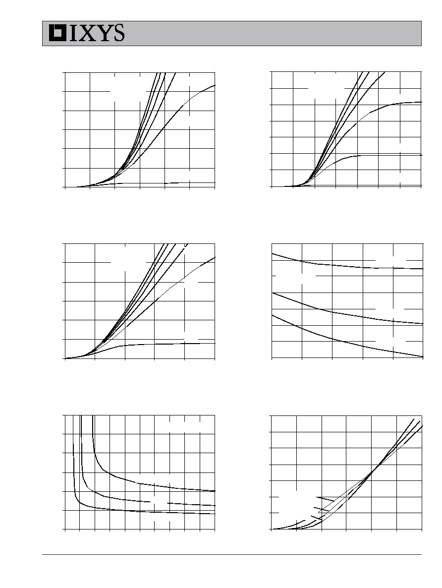
Fig. 2. Extended Output Characteristics
@ 25 deg. C
0
30
60
90
120
150
180
210
0
1
2
3
4
5
6
7
V
C E
- Volts
I
C
-
A
m
per
es
V
G E
= 1 5V
1 3V
1 1 V
9V
5V
7V
Fig. 3. Output Characteristics
@ 125 Deg. C
0
10
20
30
40
50
60
0.5
1
1.5
2
2.5
3
V
CE
- Volts
I
C
-
A
m
per
es
V
G E
= 1 5V
1 3V
1 1 V
5V
7V
9V
Fig. 1. Output Characteristics
@ 25 Deg. C
0
10
20
30
40
50
60
0.5
1
1.5
2
2.5
3
3.5
V
C E
- Volts
I
C
-
A
m
per
es
V
G E
= 1 5V
1 3V
1 1 V
7V
5V
9V
Fig. 6. Input Admittance
0
30
60
90
120
150
180
210
4
5
6
7
8
9
10
V
G E
- Volts
I
C
-
A
m
per
e
s
T
J
= 1 25
∫
C
25
∫
C
-40
∫
C
Fig. 4. Temperature Dependence of V
CE(sat)
0.6
0.7
0.8
0.9
1
1.1
1.2
1.3
25
50
75
100
125
150
T
J
- Degrees Centigrade
V
C E
(
s
a
t
)
-
N
o
r
m
a
liz
e
d
I
C
= 60A
I
C
= 30A
I
C
= 1 5A
V
G E
= 1 5V
Fig. 5. Collector-to-Emitter Voltage
vs. Gate-to-Emiiter voltage
1
1.5
2
2.5
3
3.5
4
5
6
7
8
9
10
11
12
13
14
15
V
G E
- Volts
V
C E
-
V
o
lt
s
T
J
= 25
∫
C
I
C
= 60A
30A
1 5A
IXYS reserves the right to change limits, test conditions, and dimensions.
IXYS MOSFETs and IGBTs are covered by one or more
of the following U.S. patents:
4,835,592 4,881,106 5,017,508 5,049,961 5,187,117 5,486,715 6,306,728B1 6,259,123B1 6,306,728B1
4,850,072 4,931,844 5,034,796 5,063,307 5,237,481 5,381,025 6,404,065B1 6,162,665 6,534,343
IXGR 40N60C2
IXGR 40N60C2D1
Fig. 12. Capacitance
10
100
1000
10000
0
5
10
15
20
25
30
35
40
V
C E
- Volts
Capac
i
t
anc
e
-
p
F
Cies
Coes
Cres
f = 1 M Hz
Fig. 11. Gate Charge
0
3
6
9
12
15
0
20
40
60
80
100
Q
G
- nanoCoulombs
V
G E
- V
o
l
t
s
V
C E
= 300V
I
C
= 30A
I
G
= 1 0mA
Fig. 7. Transconductance
0
10
20
30
40
50
60
70
0
30
60
90
120
150
180
I
C
- Amperes
g
f s
-
S
i
em
ens
T
J
= -40
∫
C
25
∫
C
1 25
∫
C
Fig. 8. Dependence of E
off
on R
G
0
0.2
0.4
0.6
0.8
1
1.2
1.4
1.6
1.8
2
4
6
8
10
12
14
16
R
G
- Ohms
E
of
f
-
m
illi
J
o
u
l
e
s
I
C
= 45A
I
C
= 1 5A
T
J
= 1 25
∫
C
V
G E
= 1 5V
V
C E
= 400V
I
C
= 30A
I
C
= 60A
Fig. 10. Dependence of E
off
on Temperature
0
0.2
0.4
0.6
0.8
1
1.2
1.4
1.6
25
50
75
100
125
T
J
- Degrees Centigrade
E
of
f
-
m
i
lli
J
o
u
l
e
s
I
C
= 60A
V
G E
= 1 5V
V
C E
= 400V
R
G
= 3 Ohms
R
G
= 1 0 Ohms - - - - -
I
C
= 45A
I
C
= 30A
I
C
= 1 5A
Fig. 9. Dependence of E
off
on I
c
0
0.2
0.4
0.6
0.8
1
1.2
1.4
1.6
10
20
30
40
50
60
I
C
- Amperes
E
of
f
-
M
i
l
l
i
J
oul
es
R
G
= 3 Ohms
R
G
= 1 0 Ohms - - - - -
V
G E
= 1 5V
V
C E
= 400V
T
J
= 1 25
∫
C
T
J
= 25
∫
C
© 2004 IXYS All rights reserved
IXGR 40N60C2
IXGR 40N60C2D1
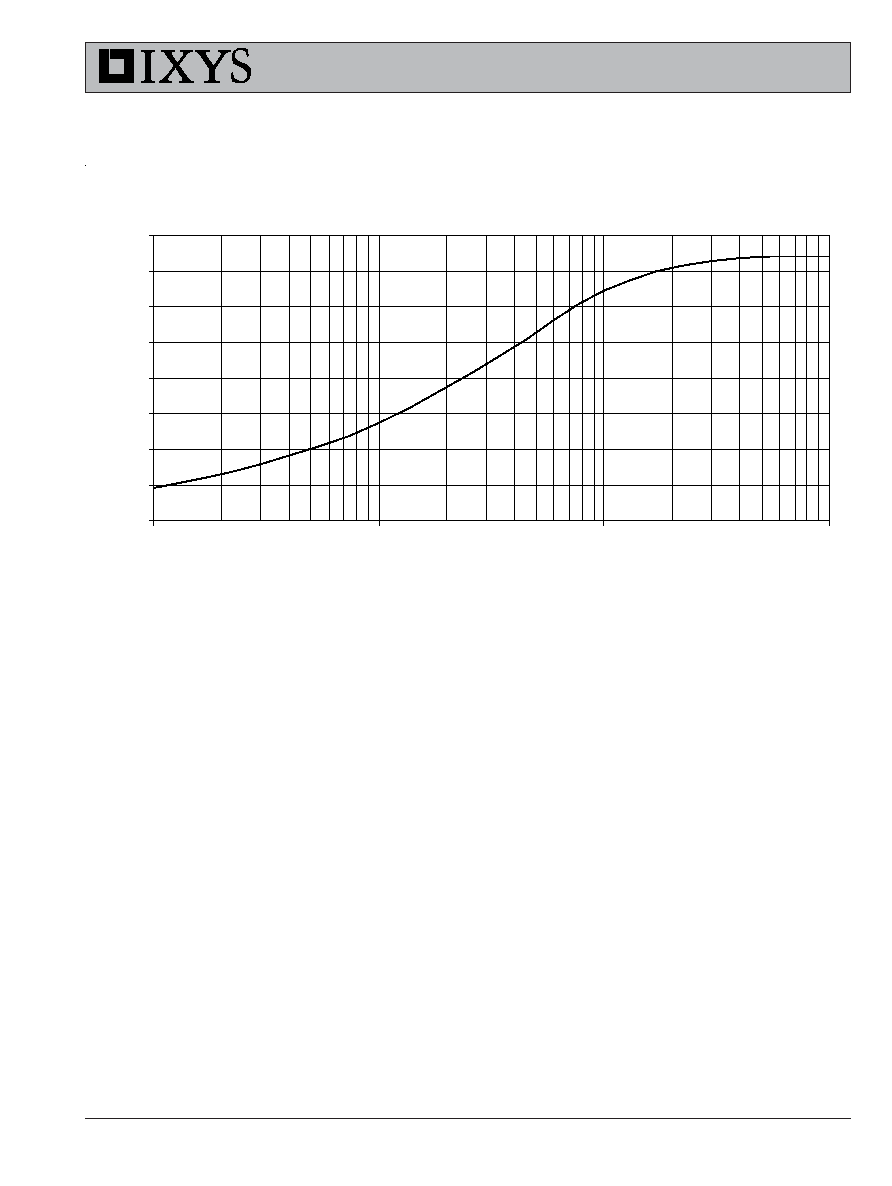
Fig. 13. Maximum Transient Thermal Resistance
0
0.1
0.2
0.3
0.4
0.5
0.6
0.7
0.8
1
10
100
1000
Pulse Width - milliseconds
R
(th) J
C
-
(∫C
/
W
)