© 2005 IXYS All rights reserved
V
CES
= 900 V
I
C25
= 64 A
V
CE(sat)
= 2.7 V
t
fi typ
= 150 ns
Symbol
Test Conditions
Characteristic Values
(T
J
= 25
∞C, unless otherwise specified)
min.
typ. max.
V
GE(th)
I
C
= 250
A, V
CE
= V
GE
3.0
5.0
V
I
CES
V
CE
= V
CES
T
J
= 25
∞C
50
A
V
GE
= 0 V
T
J
= 150
∞C
750
A
I
GES
V
CE
= 0 V, V
GE
=
±20 V
±100
nA
V
CE(sat)
I
C
= I
C110
, V
GE
= 15 V
2.2
2.7
V
T
J
= 125
∞C
2.1
V
Symbol
Test Conditions
Maximum Ratings
V
CES
T
J
= 25
∞C to 150∞C
900
V
V
CGR
T
J
= 25
∞C to 150∞C; R
GE
= 1 M
900
V
V
GES
Continuous
±20
V
V
GEM
Transient
±30
V
I
C25
T
C
= 25
∞C (limited by leads)
64
A
I
C110
T
C
= 110
∞C
32
A
I
CM
T
C
= 25
∞C, 1 ms
200
A
SSOA
V
GE
= 15 V, T
VJ
= 125
∞C, R
G
= 10
I
CM
= 64
A
(RBSOA)
Clamped inductive load @
600V
P
C
T
C
= 25
∞C
300
W
T
J
-55 ... +150
∞C
T
JM
150
∞C
T
stg
-55 ... +150
∞C
Maximum lead temperature for soldering
300
∞C
1.6 mm (0.062 in.) from case for 10 s
Plastic body for 10 s
260
∞C
M
d
Mounting torque (TO-247)
1.13/10Nm/lb.in.
Weight
TO-247
6
g
TO-268
4
g
DS99384(12/05)
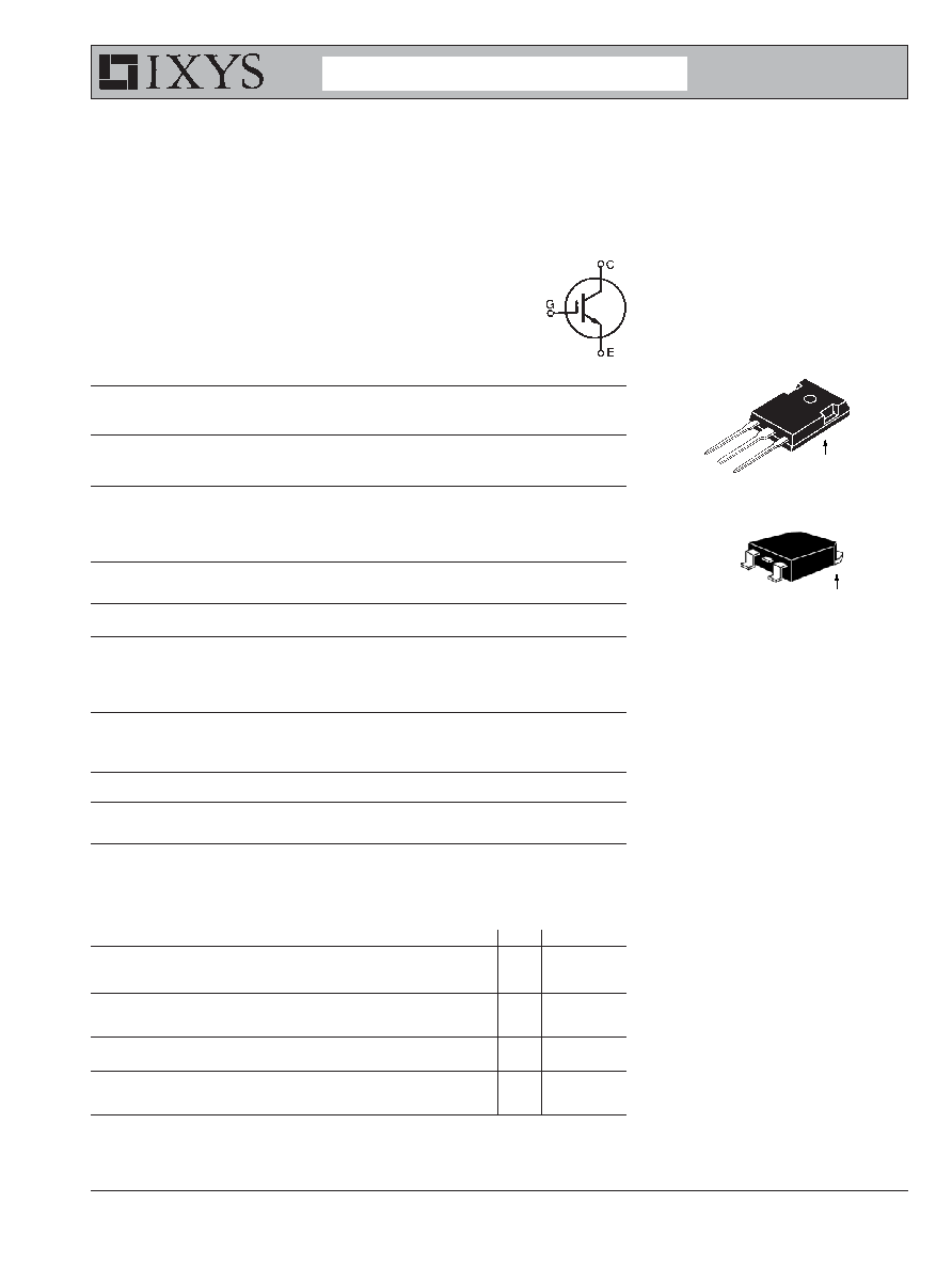
G = Gate,
C = Collector,
E = Emitter,
TAB = Collector
Features
High frequency IGBT
High current handling capability
MOS Gate turn-on
- drive simplicity
Applications
PFC circuits
Uninterruptible power supplies (UPS)
Switched-mode and resonant-mode
power supplies
AC motor speed control
DC servo and robot drives
DC choppers
Advantages
High power density
Very fast switching speeds for high
frequency applications
HiPerFAST
TM
IGBT
IXGH 32N90B2
IXGT 32N90B2
TO-268 (IXGT)
TO-247 (IXGH)
E
G
B2-Class High Speed IGBTs
Advance Technical Information
C (TAB)
G
C
E
C (TAB)
IXYS reserves the right to change limits, test conditions, and dimensions.
IXGH 32N90B2
IXGT 32N90B2
Symbol
Test Conditions
Characteristic Values
(T
J
= 25
∞C, unless otherwise specified)
min.
typ. max.
g
fs
I
C
= I
C110
A; V
CE
= 10 V,
18
28
S
Pulse test, t
300 s, duty cycle 2 %
C
ies
1790
pF
C
oes
V
CE
= 25 V, V
GE
= 0 V, f = 1 MHz
121
pF
C
res
49
pF
Q
g
89
nC
Q
ge
I
C
= I
C110
, V
GE
= 15 V, V
CE
= 0.5 V
CES
15
nC
Q
gc
34
nC
t
d(on)
20
n s
t
ri
22
n s
t
d(off)
260
400
n s
t
fi
150
n s
E
off
2.6
4.5 mJ
t
d(on)
20
n s
t
ri
22
n s
E
on
0.5
mJ
Note 1
3.8
mJ
t
d(off)
360
n s
t
fi
330
n s
E
off
5.75
mJ
R
thJC
0.42 K/W
R
thCS
(TO-247)
0.25
K/W
Inductive load, T
J
= 25
∞∞
∞∞
∞C
I
C
= I
C110
, V
GE
= 15 V
V
CE
= 720 V, R
G
= R
off
= 5
Inductive load, T
J
= 125
∞∞
∞∞
∞C
I
C
= I
C110
A, V
GE
= 15 V
V
CE
= 720 V, R
G
= R
off
= 5
TO-247 AD Outline
Dim.
Millimeter
Inches
Min.
Max.
Min.
Max.
A
4.7
5.3
.185
.209
A
1
2.2
2.54
.087
.102
A
2
2.2
2.6
.059
.098
b
1.0
1.4
.040
.055
b
1
1.65
2.13
.065
.084
b
2
2.87
3.12
.113
.123
C
.4
.8
.016
.031
D
20.80
21.46
.819
.845
E
15.75
16.26
.610
.640
e
5.20
5.72
0.205 0.225
L
19.81
20.32
.780
.800
L1
4.50
.177
P
3.55
3.65
.140
.144
Q
5.89
6.40
0.232 0.252
R
4.32
5.49
.170
.216
S
6.15 BSC
242 BSC
e
P
TO-268 Outline
Min. Recommended Footprint
(Dimensions in inches and mm)
Note 1: E
on
measured with a DSEP 30-12A ultrafast diode clamp.
IXYS MOSFETs and IGBTs are covered by
4,835,592
4,931,844
5,049,961
5,237,481
6,162,665
6,404,065 B1
6,683,344
6,727,585
one or more of the following U.S. patents:
4,850,072
5,017,508
5,063,307
5,381,025
6,259,123 B1
6,534,343
6,710,405B2
6,759,692
4,881,106
5,034,796
5,187,117
5,486,715
6,306,728 B1
6,583,505
6,710,463
6771478 B2
© 2005 IXYS All rights reserved
Fig. 2. Extended Output Characteristics
@ 25
∫
C
0
40
80
120
160
200
240
0
2
4
6
8
10
12
14
16
18
20
V
C E
- Volts
I
C
-
A
m
per
es
V
GE
= 15V
7V
9V
11V
13V
Fig. 3. Output Characteristics
@ 125
∫
C
0
10
20
30
40
50
60
70
0
0.5
1
1.5
2
2.5
3
3.5
4
4.5
V
CE
- Volts
I
C
-
A
m
per
es
V
GE
= 15V
13V
11V
9V
7V
5V
Fig. 1. Output Characteristics
@ 25
∫
C
0
10
20
30
40
50
60
70
0
0.5
1
1.5
2
2.5
3
3.5
4
4.5
V
C E
- Volts
I
C
-
A
m
per
es
V
GE
= 15V
13V
11V
9V
5V
7V
Fig. 4. Dependence of V
CE(sat)
on
Tem perature
0.7
0.8
0.9
1.0
1.1
1.2
1.3
1.4
1.5
-50
-25
0
25
50
75
100
125
150
T
J
- Degrees Centigrade
V
C E
(
s
a
t
)
- N
o
rm
a
l
i
z
e
d
I
C
= 32A
I
C
= 16A
V
GE
= 15V
I
C
= 64A
Fig. 5. Collector-to-Emitter Voltage
vs. Gate-to-Em itter voltage
1.5
2
2.5
3
3.5
4
4.5
5
5.5
6
6
7
8
9
10
11
12
13
14
15
16
17
V
G E
- Volts
V
C E
- V
o
l
t
s
T
J
= 25
∫
C
I
C
= 64A
32A
16A
Fig. 6. Input Adm ittance
0
20
40
60
80
100
120
140
4
5
6
7
8
9
10
V
G E
- Volts
I
C
-
A
m
per
es
T
J
= 125
∫
C
25
∫
C
-40
∫
C
IXGH 32N90B2
IXGT 32N90B2

IXYS reserves the right to change limits, test conditions, and dimensions.
IXGH 32N90B2
IXGT 32N90B2
Fig. 7. Transconductance
0
5
10
15
20
25
30
35
0
20
40
60
80
100
I
C
- Amperes
g
f
s
-
S
i
em
ens
T
J
=
-40
∫
C
25
∫
C
125
∫
C
Fig. 8. Gate Charge
0
2
4
6
8
10
12
14
16
0
10
20
30
40
50
60
70
80
90
100
Q
G
- nanoCoulombs
V
G E
- V
o
l
t
s
V
CE
= 450V
I
C
= 32A
I
G
= 10mA
Fig. 9. Capacitance
10
100
1000
10000
0
5
10
15
20
25
30
35
40
V
C E
- Volts
Capa
c
i
t
anc
e -
p
F
C
ies
C
oes
C
res
f = 1 MHz
Fig. 10. Reverse-Bias Safe
Operating Area
0
10
20
30
40
50
60
70
100
200
300
400
500
600
700
800
900
V
C E
- Volts
I
C
-
A
m
per
es
T
J
= 125
∫
C
R
G
= 10
dV/dT < 10V/ns
Fig. 11. Maxim um Transient Therm al Resistance
0.01
0.1
1
0.1
1
10
100
1000
Pulse Width - milliseconds
R
( t
h
) J
C
-
∫C
/
W
© 2005 IXYS All rights reserved
IXGH 32N90B2
IXGT 32N90B2
Fig. 14. Dependence of Turn-off
Energy Loss on Collector Current
0
2
4
6
8
10
12
14
16
10
20
30
40
50
60
70
I
C
- Amperes
E
o f
f
-
M
i
lliJ
o
u
l
e
s
R
G
= 5
V
GE
= 15V
V
CE
= 720V
T
J
= 125
∫
C
T
J
= 25
∫
C
Fig. 16. Dependence of Turn-off
Energy Loss on Tem perature
0
2
4
6
8
10
12
14
16
25
35
45
55
65
75
85
95
105 115 125
T
J
- Degrees Centigrade
E
o f
f
-
M
illiJ
o
u
l
e
s
I
C
= 64A
R
G
= 5
V
GE
= 15V
V
CE
= 720V
I
C
= 32A
I
C
= 16A
Fig. 12. Dependence of Turn-off
Energy Loss on Gate Resistance
0
2
4
6
8
10
12
14
16
18
0
5
10
15
20
25
30
35
40
45
50
R
G
- Ohms
E
o f
f
-
M
i
lliJ
o
u
l
e
s
I
C
= 64A
T
J
= 125
∫
C
V
GE
= 15V
V
CE
= 720V
I
C
= 32A
I
C
= 16A
Fig. 13. Dependence of Turn-on
Energy Loss on Gate Resistance
0
2
4
6
8
10
12
14
16
0
5
10
15
20
25
30
35
40
45
50
R
G
- Ohms
E
o n
-
M
i
l
l
i
J
oul
es
I
C
= 64A
T
J
= 125
∫
C
V
GE
= 15V
V
CE
= 720V
I
C
= 32A
I
C
= 16A
Fig. 15. Dependence of Turn-on
Energy Loss on Collector Current
0
1
2
3
4
5
6
7
8
9
10
20
30
40
50
60
70
I
C
- Amperes
E
o n
-
M
i
ll
i
J
oul
es
R
G
= 5
V
GE
= 15V
V
CE
= 720V
T
J
= 125
∫
C
T
J
= 25
∫
C
Fig. 17. Dependence of Turn-on
Energy Loss on Tem perature
0
1
2
3
4
5
6
7
8
9
10
25
35
45
55
65
75
85
95
105
115 125
T
J
- Degrees Centigrade
E
o n
-
M
i
ll
i
J
oul
es
I
C
= 64A
R
G
= 5
V
GE
= 15V
V
CE
= 720V
I
C
= 32A
I
C
= 16A

IXYS reserves the right to change limits, test conditions, and dimensions.
IXGH 32N90B2
IXGT 32N90B2
Fig. 18. Dependence of Turn-off
Sw itching Tim e on Gate Resistance
350
375
400
425
450
475
500
525
550
4
6
8
10
12
14
16
18
20
R
G
- Ohms
t
d
(
o
f f
)
-
N
anos
ec
onds
320
330
340
350
360
370
380
390
400
t
f i
-
Nano
s
e
c
onds
t
d(off)
t
fi
- - - - -
T
J
= 125∫C, V
GE
= 15V
V
CE
= 720V
I
C
= 32A, 16A
I
C
= 16A, 32A, 64A
Fig. 20. Dependence of Turn-off
Sw itching Time
on Collector Current
100
150
200
250
300
350
400
450
500
15
20
25
30
35
40
45
50
55
60
65
I
C
- Amperes
t
d
(
o f
f
)
/
t
f i
-
N
anos
ec
o
nds
t
d(off)
t
fi
- - - - -
R
G
= 5, V
GE
= 15V
V
CE
= 720V
T
J
= 125
∫
C
T
J
= 25
∫
C
Fig. 22. Dependence of Turn-off
Sw itching Tim e on Tem perature
100
150
200
250
300
350
400
25
35
45
55
65
75
85
95
105 115 125
T
J
- Degrees Centigrade
t
d (
o
f
f
)
/
t
f i
-
N
a
n
o
se
co
n
d
s
t
d(off)
t
fi
- - - - -
R
G
= 5 , V
GE
= 15V
V
CE
= 720V
I
C
= 64A, 32A, 16A
I
C
= 64A, 32A, 16A
Fig. 19. Dependence of Turn-on
Sw itching Time on Gate Resistance
15
20
25
30
35
40
45
4
6
8
10
12
14
16
18
20
R
G
- Ohms
t
d
(
o
n
)
-
Na
nos
ec
on
ds
0
30
60
90
120
150
180
t
r i
-
Nanos
ec
onds
t
d(on)
t
ri
- - - - -
T
J
= 125∫C, V
GE
= 15V
V
CE
= 720V
I
C
= 32A
I
C
= 16A
I
C
= 64A
Fig. 21. Dependence of Turn-on
Sw itching Tim e
on Collector Current
10
12
14
16
18
20
22
24
26
28
30
10
20
30
40
50
60
70
I
C
- Amperes
t
d (
o
n
)
-
N
a
nos
e
c
o
nds
0
10
20
30
40
50
60
70
80
90
100
t
r i
-
N
a
n
o
se
co
n
d
s
t
d(on)
t
ri
- - - -
R
G
= 5, V
GE
= 15V
V
CE
= 720V
T
J
= 125
∫
C
T
J
= 25
∫
C
Fig. 23. Dependence of Turn-on
Sw itching Time on Temperature
10
15
20
25
30
35
40
25
35
45
55
65
75
85
95 105 115 125
T
J
- Degrees Centigrade
t
d
(
o n )
-
Nanos
e
c
onds
0
25
50
75
100
125
150
t
r i
-
Nano
s
e
c
ond
s
t
d(on)
t
ri
- - - - -
R
G
= 5 , V
GE
= 15V
V
CE
= 720V
I
C
= 32A
I
C
= 64A
I
C
= 1 6A

© 2005 IXYS All rights reserved
ADVANCE TECHNICAL INFORMATION
The product presented herein is under development. The Technical Specifications offered
are derived from a subjective evaluation of the design, based upon prior knowledge and
experience, and constitute a "considered reflection" of the anticipated objective result.
IXYS reserves the right to change limits, test conditions, and dimensions without notice.