© 2003 IXYS All rights reserved
Symbol
Test Conditions
Maximum Ratings
V
DSS
T
J
= 25
∞C to 150∞C
600
V
V
GS
Continuous
±20
V
I
D25
T
C
= 25
∞C; Note 1
85
A
I
D100
T
C
= 100
∞C, Note 1
55
A
I
D(RMS)
Package lead current limit
75
A
E
AS
I
o
= 10A, T
C
= 25
∞C
1.8
J
P
D
T
C
= 25
∞C
700
W
T
J
-55 ... +150
∞C
T
JM
150
∞C
T
stg
-55 ... +125
∞C
T
L
1.6 mm (0.062 in.) from case for 10 s
300
∞C
M
d
Mounting torque
1.2 / 10
Nm/lb-in
Weight
10
g
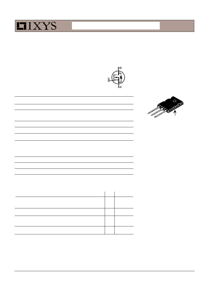
G = Gate
D = Drain
S = Source
DS99065B(08/03)
ADVANCE TECHNICAL INFORMATION
Power MOSFET
Low R
DS(on)
, High Voltage,
CoolMOS
TM
Superjunction MOSFET
IXKK 85N60C
V
DSS
= 600 V
I
D25
=
85
A
R
DS(on)
= 36 m
Features
3
RD
generation CoolMOS power MOSFET
- High blocking capability
- Low on resistance
- Avalanche rated for unclamped inductive
switching (UIS)
Low thermal resistance due to reduced
chip thickness
Applications
Switched Mode Power Supplies (SMPS)
Uninterruptible Power Supplies (UPS)
Power Factor Correction (PFC)
Welding
Inductive Heating
S
G
D
(TAB)
TO-264
CoolMos is a trademark of Infineon
Technology.
IXYS reserves the right to change limits, test conditions, and dimensions.
Symbol
Test Conditions
Characteristic Values
(T
J
= 25
∞C, unless otherwise specified)
min.
typ. max.
R
DS(on)
V
GS
= 10 V, I
D
= I
D100
, Note
30
36 m
V
GS
= 10 V, I
D
= I
D100
, Note T
J
= 125
∞C
75
m
V
GS(th)
V
DS
= V
GS
, I
D
= 4 mA
2
4
V
I
DSS
V
DS
= V
DSS
T
J
= 25
∞C
50
µA
V
GS
= 0 V
T
J
= 150
∞C
400
µA
I
GSS
V
GS
=
±20 V
DC
, V
DS
= 0
±200
nA
© 2003 IXYS All rights reserved
Symbol
Test Conditions
Characteristic Values
(T
J
= 25
∞C, unless otherwise specified)
min.
typ. max.
g
FS
V
DS
= 10 V, I
D
= I
D100
90
S
Q
g(on)
540 650
nC
Q
gs
V
GS
= 10 V, V
DS
= 350 V, I
D
= 40 A
60
nC
Q
gd
220
nC
t
d(on)
20
ns
t
r
V
GS
= 10 V, V
DS
= 380V
27
ns
t
d(off)
I
D
= 60 A, R
G
= 2.2
14
ns
t
f
10
ns
R
thJC
0.18
K/W
R
thCH
0.15
K/W
Reverse Correction
Characteristic Values
(T
J
= 25
∞C, unless otherwise specified)
Symbol
Test Conditions
min.
typ. max.
V
SD
I
F
= I
D100
, V
GS
= 0 V
1.0
1.2
V
Note 1
Note: 1. Pulse test, t
100
300 µs, duty cycle d 2 %
IXKK 85N60C
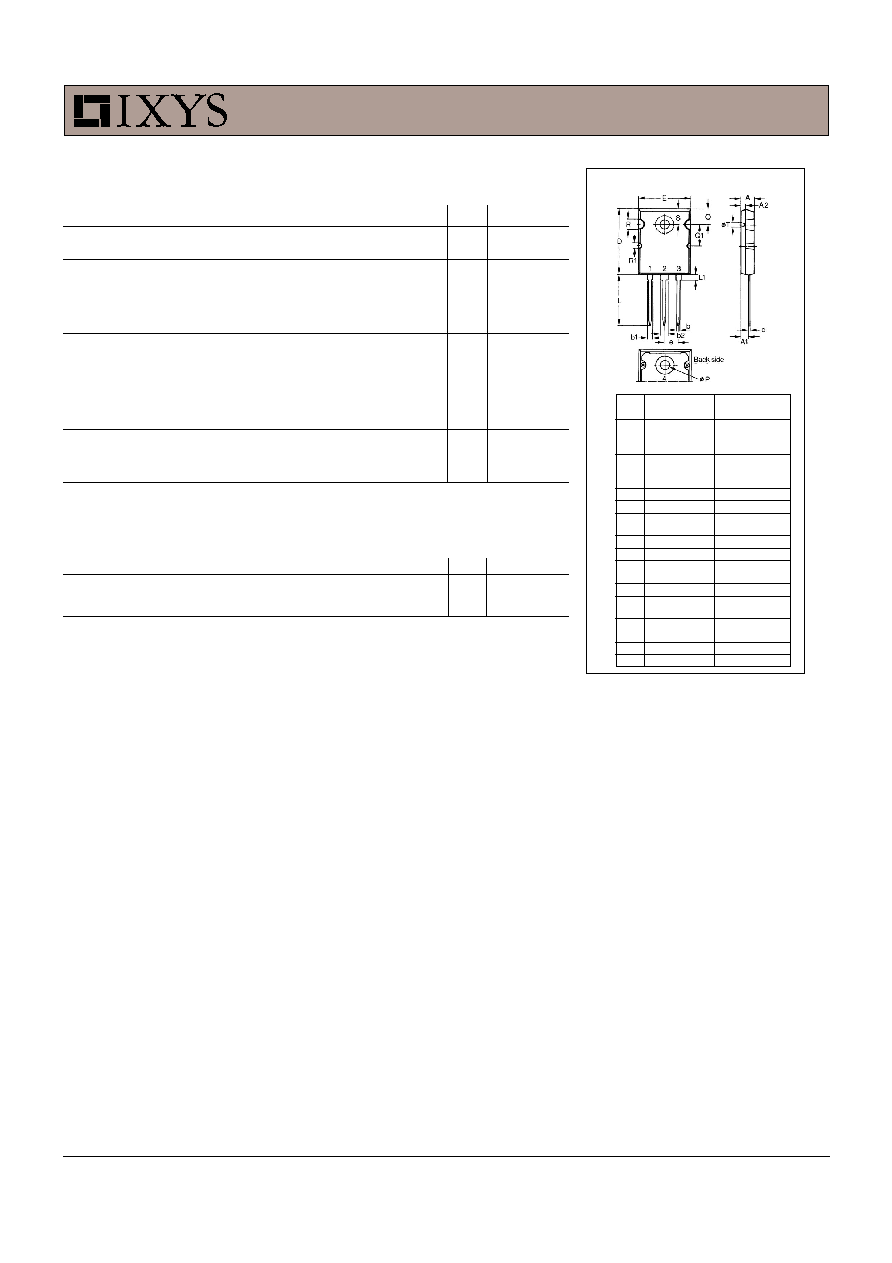
TO-264 Outline
Millimeter
Inches
Min.
Max.
Min.
Max.
A
4.82
5.13
.190
.202
A1
2.54
2.89
.100
.114
A2
2.00
2.10
.079
.083
b
1.12
1.42
.044
.056
b1
2.39
2.69
.094
.106
b2
2.90
3.09
.114
.122
c
0.53
0.83
.021
.033
D
25.91
26.16
1.020
1.030
E
19.81
19.96
.780
.786
e
5.46 BSC
.215 BSC
J
0.00
0.25
.000
.010
K
0.00
0.25
.000
.010
L
20.32
20.83
.800
.820
L1
2.29
2.59
.090
.102
P
3.17
3.66
.125
.144
Q
6.07
6.27
.239
.247
Q1
8.38
8.69
.330
.342
R
3.81
4.32
.150
.170
R1
1.78
2.29
.070
.090
S
6.04
6.30
.238
.248
T
1.57
1.83
.062
.072
Dim.
© 2003 IXYS All rights reserved
IXKK 85N60C
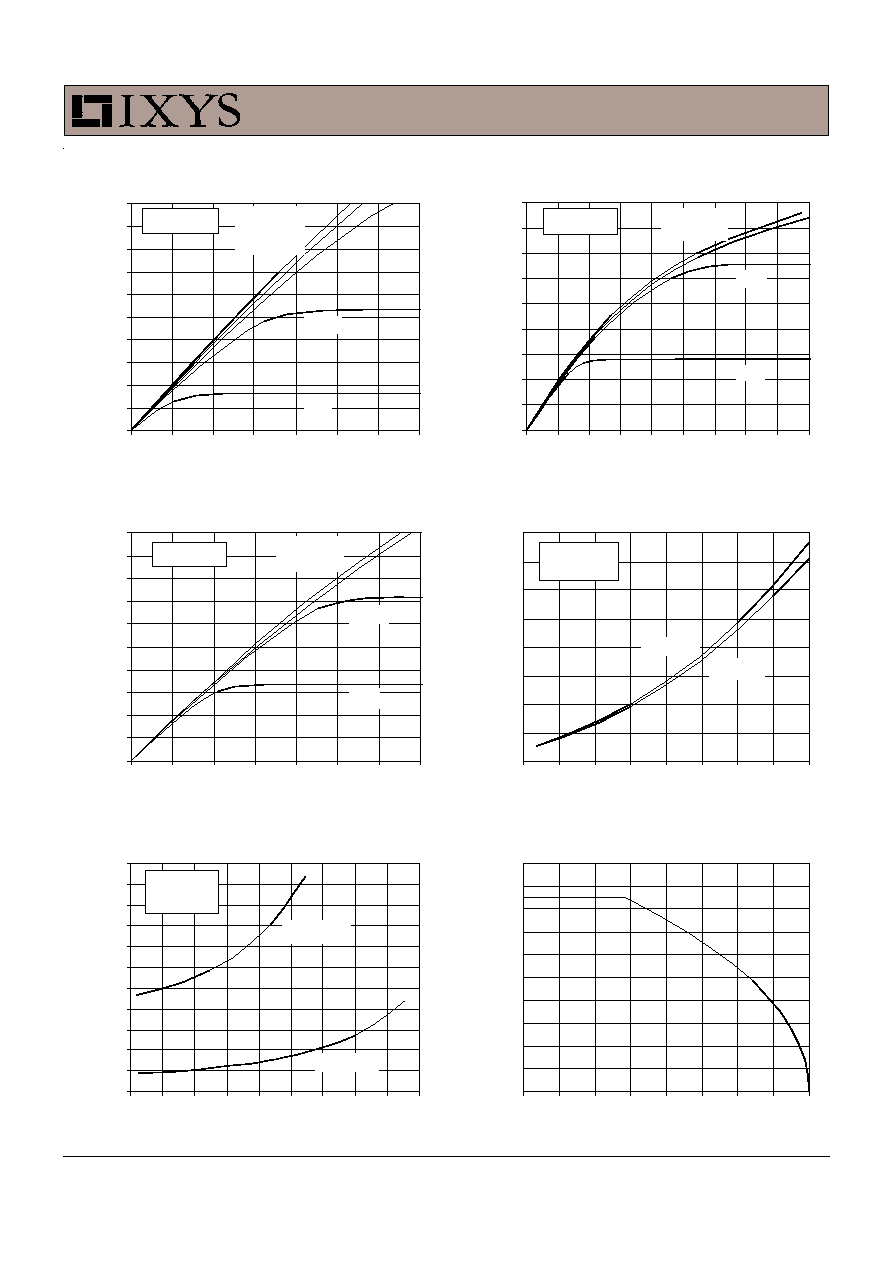
Fig. 2. Extended Output Characteristics
@ 25 deg. C
0
40
80
120
160
200
240
280
320
360
0
2
4
6
8
10
12
14
16
18
V
D S
- Volts
I
D
- A
m
p
e
re
s
V
GS
= 10V
7V
5V
6V
t
p = 300µs
Fig. 3. Output Characteristics
@ 125 Deg. C
0
10
20
30
40
50
60
70
80
90
100
0
1
2
3
4
5
6
7
V
D S
- Volts
I
D
-
A
m
per
es
V
GS
= 10V
5V
4V
4.5V
t
p = 300µs
Fig. 1. Output Characteristics
@ 25 Deg. C
0
10
20
30
40
50
60
70
80
90
100
0
0.5
1
1.5
2
2.5
3
3.5
V
D S
- Volts
I
D
-
A
m
per
e
s
V
GS
= 10V
6V
5V
4V
4.5V
t
p = 300µs
Fig. 4. R
DS(on)
Norm alized to I
D100
Value
vs. Junction Tem perature
0.4
0.7
1
1.3
1.6
1.9
2.2
2.5
2.8
-50
-25
0
25
50
75
100
125
150
T
J
- Degrees Centigrade
R
D
S
(
on)
- N
o
rm
a
l
i
z
e
d
I
D
= 60A
I
D
= 30A
V
GS
= 10V
t
p = 300µs
Fig. 6. Drain Current vs. Case
Tem perature
0
10
20
30
40
50
60
70
80
90
100
-50
-25
0
25
50
75
100
125
150
T
C
- Degrees Centigrade
I
D
-
A
m
per
e
s
Fig. 5. R
DS(on)
Norm alized to
I
D100
Value vs. I
D
0.7
1
1.3
1.6
1.9
2.2
2.5
2.8
3.1
3.4
3.7
4
0
40
80
120
160
200
240
280
320
360
I
D
- Amperes
R
D
S
(
on)
- N
o
rm
a
l
i
z
e
d
T
J
= 125∫C
T
J
= 25∫C
V
GS
= 10V
t
p = 300µs

© 2003 IXYS All rights reserved
IXKK 85N60C
Fig. 11. Capacitance
10
100
1000
10000
100000
0
10
20
30
40
50
60
70
80
90
100
V
DS
- Volts
C
a
pa
c
i
t
an
c
e -
p
F
C
iss
C
oss
C
rss
f = 1MHz
Fig. 10. Gate Charge
0
1
2
3
4
5
6
7
8
9
10
0
60
120
180
240
300
360
420
480
540
Q
G
- nanoCoulombs
V
G S
- V
o
l
t
s
V
DS
= 350V
I
D
= 80A
I
G
= 10mA
Fig. 7. Input Adm ittance
0
30
60
90
120
150
180
210
240
2
2.5
3
3.5
4
4.5
5
5.5
6
V
G S
- Volts
I
D
- A
m
p
e
re
s
T
J
= 125∫C
25∫C
-40∫C
Fig. 12. Maxim um Transient Therm al
Resistance
0
0.02
0.04
0.06
0.08
0.1
0.12
0.14
0.16
0.18
1
10
100
1000
Pulse Width - milliseconds
R
(t
h
) J
C
-
(∫
C
/
W
)
Fig. 8. Transconductance
0
20
40
60
80
100
120
140
160
180
0
30
60
90
120
150
180
210
240
I
D
- Amperes
g
f s
-
S
i
e
m
e
n
s
T
J
= -40∫C
25∫C
125∫C
Fig. 9. Source Current vs. Source-To-
Drain Voltage
0
20
40
60
80
100
120
140
160
180
200
0.4
0.5
0.6
0.7
0.8
0.9
1
1.1
V
S D
- Volts
I
S
-
A
m
per
es
T
J
= 125∫C
T
J
= 25∫C