
© 2002 IXYS All rights reserved
Symbol
Test Conditions
Characteristic Values
(T
J
= 25
∞
C, unless otherwise specified)
Min.
Typ.
Max.
BV
CES
I
C
= 250
µ
A, V
GE
= 0 V
1200
V
V
GE(th)
I
C
= 250
µ
A, V
CE
= V
GE
3
6
V
I
CES
V
CE
= V
CES
T
J
= 25
∞
C
50
µ
A
V
GE
= 0 V
T
J
= 125
∞
C
2.5
mA
I
GES
V
CE
= 0 V, V
GE
=
±
20 V
±
100
nA
V
CE(sat)
I
C
= I
CE90
, V
GE
= 15
3.0
3.4
V
T
J
= 125
∞
C
2.8
V
98922 (5/02)
Features
∑
International standard packages
JEDEC TO-220AB and TO-263AA
∑
Low switching losses, low V
(sat)
∑
MOS Gate turn-on
- drive simplicity
Applications
∑
AC motor speed control
∑
DC servo and robot drives
∑
DC choppers
∑
Uninterruptible power supplies (UPS)
∑
Switch-mode and resonant-mode
power supplies
Advantages
∑
Easy to mount with one screw
∑
Reduces assembly time and cost
∑
High power density
G
E
C (TAB)
TO-263 AA (IXSA)
G C
E
TO-220AB (IXSP)
Advance Technical Information
V
CES
=1200 V
I
C25
= 30 A
V
CE(sat)
= 3.4 V
IXSA 15N120B
IXSP 15N120B
HIGH Voltage IGBT
"S" Series - Improved SCSOA Capability
Symbol
Test Conditions
Maximum Ratings
V
CES
T
J
= 25
∞
C to 150
∞
C
1200
V
V
CGR
T
J
= 25
∞
C to 150
∞
C; R
GE
= 1 M
1200
V
V
GES
Continuous
±
20
V
V
GEM
Transient
±
30
V
I
C25
T
C
= 25
∞
C
30
A
I
C90
T
C
= 90
∞
C
15
A
I
CM
T
C
= 25
∞
C, 1 ms
60
A
SSOA
V
GE
= 15 V, T
J
= 125
∞
C, R
G
= 10
I
CM
= 40
A
(RBSOA)
Clamped inductive load
@ 0.8 V
CES
t
SC
T
J
= 125
∞
C, V
GE
= 720 V; V
GE
= 15 V, R
G
= 10
10
µ
s
Non repetitive
P
C
T
C
= 25
∞
C
150
W
T
J
-55 ... +150
∞
C
T
JM
150
∞
C
T
stg
-55 ... +150
∞
C
M
d
Mounting torque
(TO-247)
1.13/10 Nm/lb.in.
Maximum lead temperature for soldering
300
∞
C
1.6 mm (0.062 in.) from case for 10 s
Maximum tab temperature for soldering (TO-263)
260
∞
C
Weight
TO-220
4
g
TO-263
2
g
C (TAB)
IXYS reserves the right to change limits, test conditions, and dimensions.
IXYS MOSFETs and IGBTs are covered by one or more of the following U.S. patents:
4,835,592
4,881,106
5,017,508
5,049,961
5,187,117
5,486,715
6,306,728B1
4,850,072
4,931,844
5,034,796
5,063,307
5,237,481
5,381,025
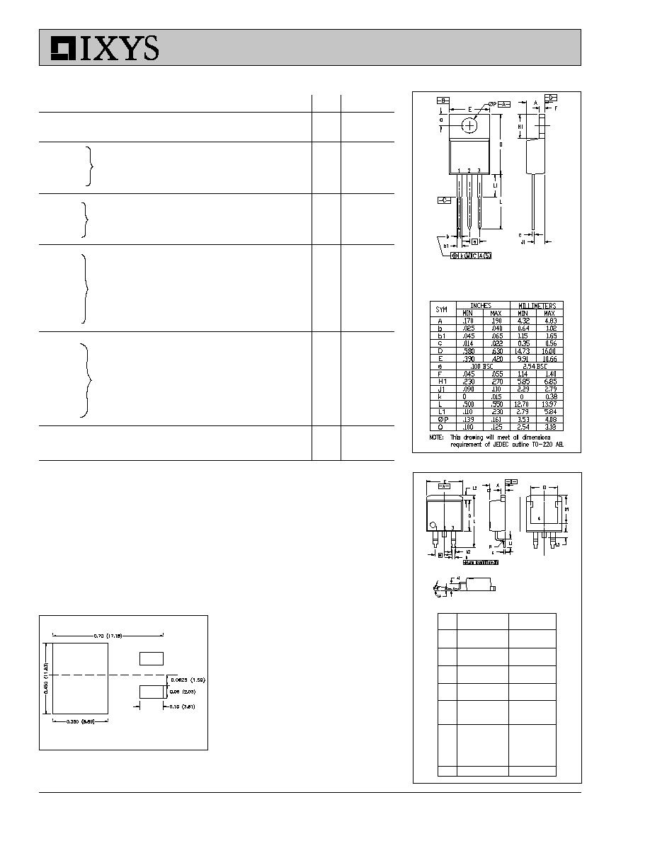
TO-263 AA Outline
1. Gate
2. Collector
3. Emitter
4. Collector
Bottom Side
Dim.
Millimeter
Inches
Min.
Max.
Min.
Max.
A
4.06
4.83
.160
.190
A1
2.03
2.79
.080
.110
b
0.51
0.99
.020
.039
b2
1.14
1.40
.045
.055
c
0.46
0.74
.018
.029
c2
1.14
1.40
.045
.055
D
8.64
9.65
.340
.380
D1
7.11
8.13
.280
.320
E
9.65
10.29
.380
.405
E1
6.86
8.13
.270
.320
e
2.54
BSC
.100
BSC
L
14.61
15.88
.575
.625
L1
2.29
2.79
.090
.110
L2
1.02
1.40
.040
.055
L3
1.27
1.78
.050
.070
L4
0
0.38
0
.015
R
0.46
0.74
.018
.029
Pins: 1 - Gate
2 - Collector
3 - Emitter
4 - Collector
Bottom Side
TO-220 AB Dimensions
Symbol
Test Conditions
Characteristic Values
(T
J
= 25
∞
C, unless otherwise specified)
Min. Typ.
Max.
g
fs
I
C
= I
C90
; V
CE
= 10 V,
7
9.5
S
Note2
C
ies
1400
pF
C
oes
V
CE
= 25 V, V
GE
= 0 V, f = 1 MHz
98
pF
C
res
37
pF
Q
g
57
nC
Q
ge
I
C
= I
C90
, V
GE
= 15 V, V
CE
= 0.5 V
CES
14
nC
Q
gc
25
nC
t
d(on)
30
ns
t
ri
25
ns
t
d(off)
148
280
ns
t
fi
160
320
ns
E
off
1.75
3.0
mJ
t
d(on)
30
ns
t
ri
25
ns
E
on
1.1
mJ
t
d(off)
265
ns
t
fi
298
ns
E
off
3.1
mJ
R
thJC
0.83
K/W
R
thCK
TO-220
0.5
K/W
Inductive load, T
J
= 25
∞∞
∞∞
∞
C
I
C
= I
C90
, V
GE
= 15 V
V
CE
= 960 V, R
G
= R
off
= 10
Note3
Inductive load, T
J
= 125
∞∞
∞∞
∞
C
I
C
= I
C90
, V
GE
= 15 V
V
CE
= 960 V, R
G
= R
off
= 10
Note3
IXSA 15N120B
IXSP 15N120B
Min. Recommended Footprint
(Dimensions in inches and mm)
Notes: 1.
Device must be heatsunk for high temperature leakage current
measurements to avoid thermal runaway.
2.
Pulse test, t
300
µ
s, duty cycle
2 %
3.
Switching times may increase for V
CE
(Clamp) > 0.8 V
CES
, higher T
J
or
increased R
G
.