DS99249(10/04)
Features
∑ International standard package
∑ Guaranteed Short Circuit SOA
capability
∑ Low V
CE(sat)
- for low on-state conduction losses
∑ High current handling capability
∑ MOS Gate turn-on
- drive simplicity
∑ Fast fall time for switching speeds
up to 20 kHz
Applications
∑ AC motor speed control
∑ Uninterruptible power supplies (UPS)
∑ Welding
Advantages
∑ High power density
IXSH 30N60B2D1
IXST 30N60B2D1
High Speed IGBT
with Diode
Short Circuit SOA Capability
Symbol
Test Conditions
Maximum Ratings
V
CES
T
J
= 25
∞C to 150∞C
600
V
V
CGR
T
J
= 25
∞C to 150∞C; R
GE
= 1 M
600
V
V
GES
Continuous
± 20
V
V
GEM
Transient
± 30
V
I
C25
T
C
= 25
∞C
48
A
I
C110
T
C
= 110
∞C
30
A
I
F(110)
28
A
I
CM
T
C
= 25
∞C, 1 ms
90
A
SSOA
V
GE
= 15 V, T
J
= 125
∞C, R
G
= 10
I
CM
= 48
A
(RBSOA)
Clamped inductive load
@ 0.8 V
CES
t
SC
V
GE
= 15 V, V
CE
= 360 V, T
J
= 125
∞C
10
µs
(SCSOA)
R
G
= 10
, non repetitive
P
C
T
C
= 25
∞C
250
W
T
J
-55 ... +150
∞C
T
JM
150
∞C
T
stg
-55 ... +150
∞C
Weight
TO-247
6
g
TO-268
5
g
Maximum lead temperature for soldering
300
∞C
1.6 mm (0.062 in.) from case for 10 s
Maximum tab temperature for soldering for 10s
260
∞C
Symbol
Test Conditions
Characteristic Values
(T
J
= 25
∞C, unless otherwise specified)
min.
typ.
max.
V
GE(th)
I
C
= 750
µA, V
CE
= V
GE
4.0
7.0
V
I
CES
V
CE
= V
CES
150
µA
V
GE
= 0 V
1
mA
I
GES
V
CE
= 0 V, V
GE
=
± 20 V
± 100
nA
V
CE(sat)
I
C
= 24A, V
GE
= 15 V
2.5
V
Preliminary Data Sheet
V
CES
= 600 V
I
C25
= 48 A
V
CE(sat)
= 2.5 V
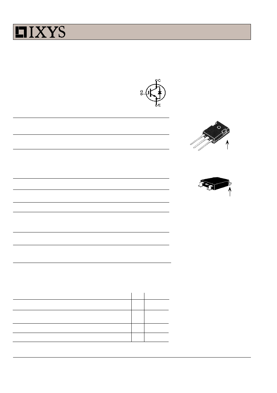
G = Gate
C = Collector
E = Emitter
TAB = Collector
TO-247 (IXSH)
© 2004 IXYS All rights reserved
TO-268 (IXST)
G
E
C (TAB)
G
C E
C (TAB)
IXSH 30N60B2D1
IXST 30N60B2D1
Reverse Diode (FRED)
Characteristic Values
(T
J
= 25
∞C, unless otherwise specified)
Symbol
Test Conditions
min.
typ. max.
V
F
I
F
= 30A, V
GE
= 0 V
T
J
=150
∞C
1.6
V
2.5
V
I
RM
I
F
= 50A, V
GE
= 0 V, -di
F
/dt = 100 A/
µs T
J
= 100
∞C 2.0
2.5
A
t
rr
V
R
= 100 V
T
J
= 100
∞C 150
ns
t
rr
I
F
= 1 A; -di/dt = 100 A/
µs; V
R
= 30 V
30
ns
R
thJC
0.9 K/W
Symbol
Test Conditions
Characteristic Values
(T
J
= 25
∞C, unless otherwise specified)
min. typ. max.
g
fs
I
C
= 24A; V
CE
= 10 V, Note 1
7.0
12.0
S
C
ies
1220
pF
C
oes
V
CE
= 25 V, V
GE
= 0 V
110
pF
f = 1 MHz
20N60B2D1
140
pF
C
res
42
pF
Q
g
50
nC
Q
ge
I
C
= 24A, V
GE
= 15 V, V
CE
= 0.5 V
CES
23
nC
Q
gc
15
nC
t
d(on)
30
ns
t
ri
30
ns
t
d(off)
130
280
ns
t
fi
140
300
ns
E
off
0.55
1.0 mJ
t
d(on)
30
ns
t
ri
50
ns
E
on
20N60B2
0.32
mJ
20N60B2D1
0.82
mJ
t
d(off)
202
ns
t
fi
234
ns
E
off
1.18
mJ
R
thJC
0.50 K/W
R
thCS
0.21
K/W
Inductive load, T
J
= 25
∞∞
∞∞
∞C
I
C
= 24A, V
GE
= 15 V
V
CE
= 400 V, R
G
= 5
Switching times may increase for V
CE
(Clamp) > 0.8 ∑ V
CES
, higher T
J
or
increased R
G
Inductive load, T
J
= 125
∞∞
∞∞
∞C
I
C
= 24 A, V
GE
= 15 V
V
CE
= 400 V, R
G
= 5
Switching times may increase for
V
CE
(Clamp) > 0.8 ∑ V
CES
, higher T
J
or increased R
G
Note 1:
Pulse test, t
300 µs, duty cycle d 2 %
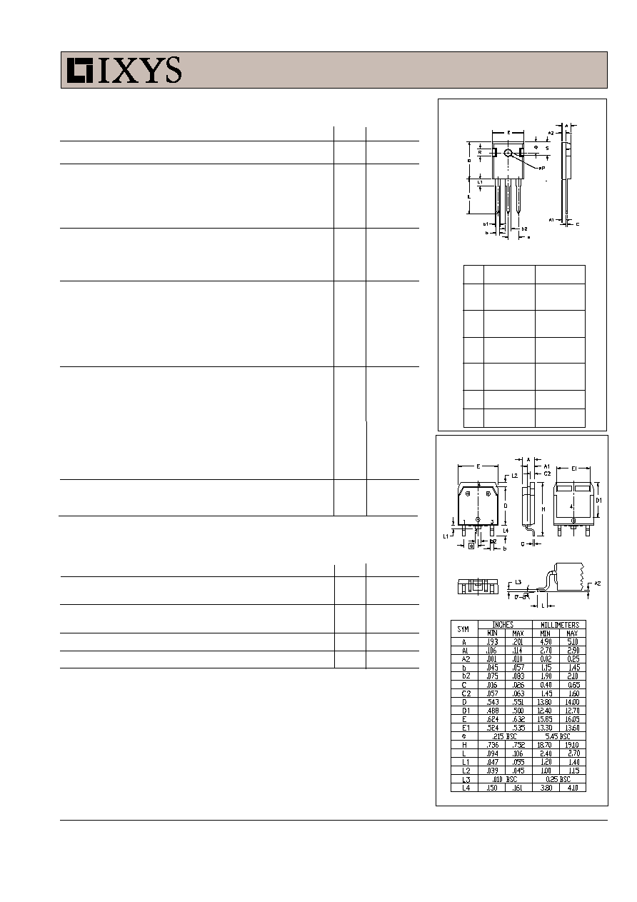
TO-247 (IXSH) Outline
Dim.
Millimeter
Inches
Min.
Max.
Min. Max.
A
4.7
5.3
.185
.209
A
1
2.2
2.54
.087
.102
A
2
2.2
2.6
.059
.098
b
1.0
1.4
.040
.055
b
1
1.65
2.13
.065
.084
b
2
2.87
3.12
.113
.123
C
.4
.8
.016
.031
D
20.80
21.46
.819
.845
E
15.75
16.26
.610
.640
e
5.20
5.72
0.205 0.225
L
19.81
20.32
.780
.800
L1
4.50
.177
P
3.55
3.65
.140
.144
Q
5.89
6.40
0.232 0.252
Terminals: 1 - Gate
2 - Drain
1 2 3
TO-268 (IXST) Outline
IXYS MOSFETs and IGBTs are covered by
4,835,592
4,931,844
5,049,961
5,237,481
6,162,665
6,404,065 B1
6,683,344
6,727,585
one or moreof the following U.S. patents:
4,850,072
5,017,508
5,063,307
5,381,025
6,259,123 B1
6,534,343
6,710,405B2
6,759,692
4,881,106
5,034,796
5,187,117
5,486,715
6,306,728 B1
6,583,505
6,710,463
IXSH 30N60B2D1
IXST 30N60B2D1
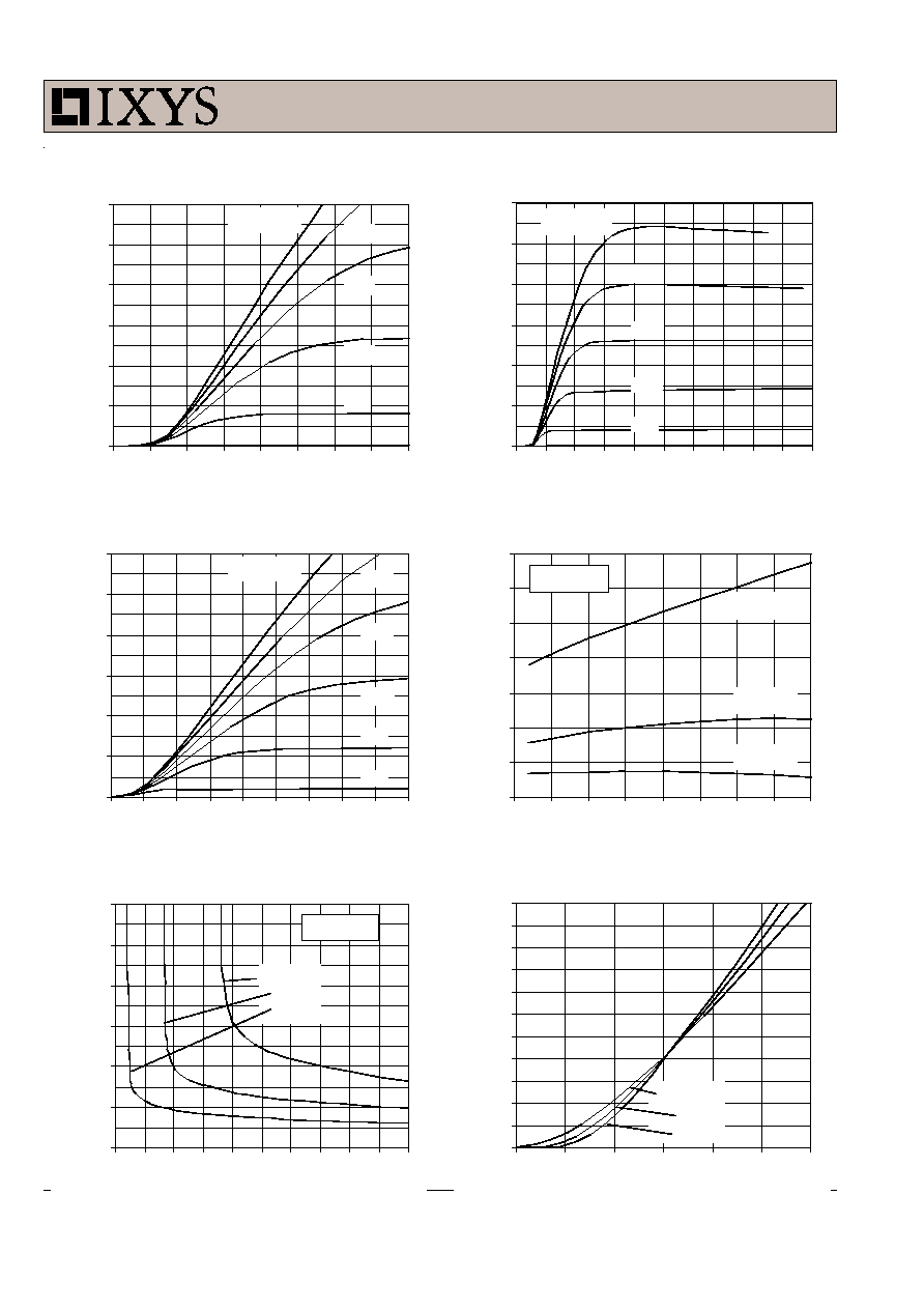
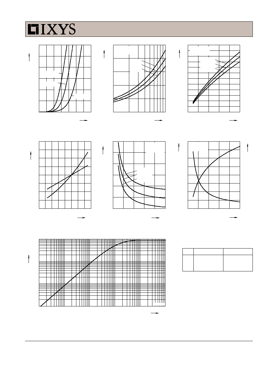
Fig. 2. Extended Output Characteristics
@ 25
∫
C
0
20
40
60
80
100
120
0
2
4
6
8
10
12
14
16
18
20
V
C E
- Volts
I
C
-
A
m
p
e
re
s
V
GE
= 17V
9V
11V
13V
15V
Fig. 3. Output Characteristics
@ 125
∫
C
0
10
20
30
40
50
60
0.5
1
1.5
2
2.5
3
3.5
4
4.5
5
V
CE
- Volts
I
C
- A
m
p
e
r
e
s
V
GE
= 17V
9V
7V
11V
13V
15V
Fig. 1. Output Characteristics
@ 25
∫
C
0
10
20
30
40
50
60
0.5
1
1.5
2
2.5
3
3.5
4
4.5
V
C E
- Volts
I
C
- A
m
p
e
r
e
s
V
GE
= 17V
9V
11V
13V
15V
Fig. 4. Dependence of V
CE(sat)
on
Tem perature
0.6
0.8
1.0
1.2
1.4
1.6
1.8
2.0
-50
-25
0
25
50
75
100
125
150
T
J
- Degrees Centigrade
V
C E
(
s
a
t
)
- N
o
rm
a
l
i
z
e
d
I
C
= 24A
I
C
= 12A
V
GE
= 15V
I
C
= 48A
Fig. 5. Collector-to-Em itter Voltage
vs. Gate-to-Em itter voltage
1
2
3
4
5
6
7
9
10
11
12
13
14
15
16
17
18
19
V
G E
- Volts
V
C E
- V
o
l
t
s
T
J
= 25
∫
C
I
C
= 48A
24A
12A
Fig. 6. Input Adm ittance
0
10
20
30
40
50
60
70
80
90
100
110
6
8
10
12
14
16
18
V
G E
- Volts
I
C
- A
m
p
e
r
e
s
T
J
= 125
∫
C
25
∫
C
-40
∫
C
IXSH 30N60B2D1
IXST 30N60B2D1
Fig. 7. Transconductance
0
2
4
6
8
10
12
14
16
18
0
20
40
60
80
100
120
I
C
- Amperes
g
f
s
-
S
i
em
en
s
T
J
= -40
∫
C
25
∫
C
125
∫
C
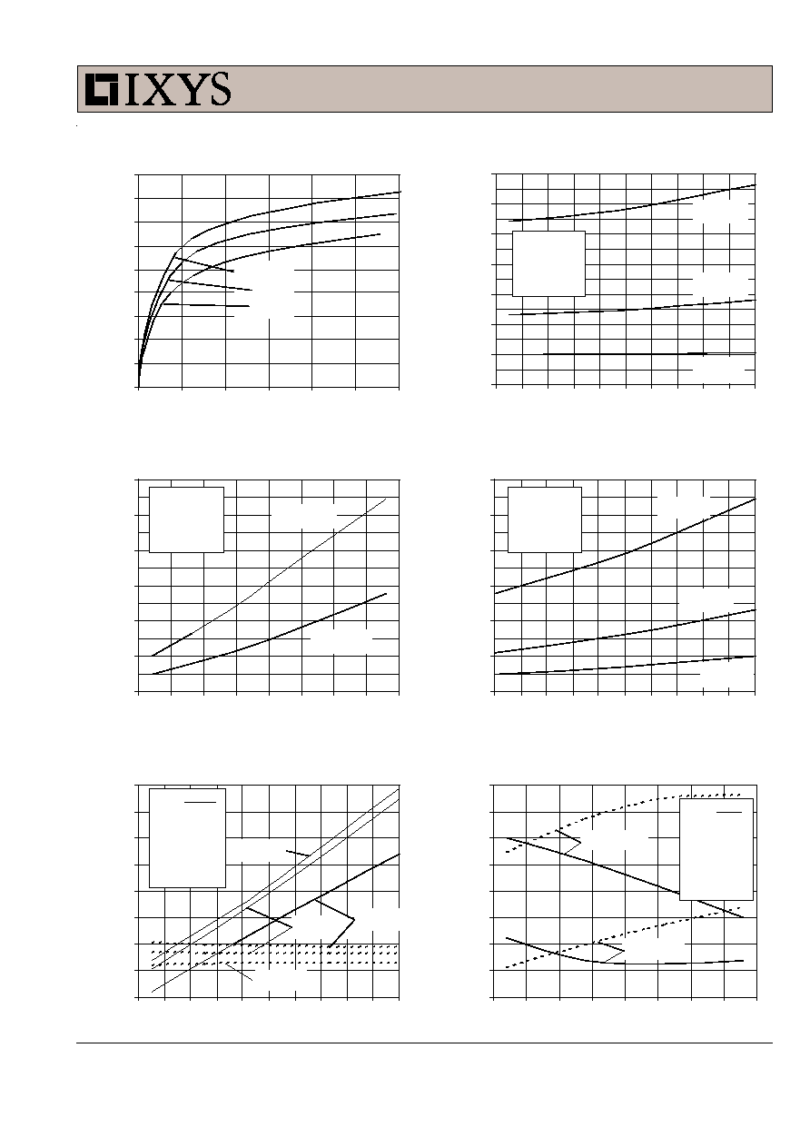
Fig. 8. Dependence of Turn-off
Energy Loss on R
G
0.0
0.5
1.0
1.5
2.0
2.5
3.0
3.5
0
10
20
30
40
50
60
70
80
90
100
R
G
- Ohms
E
o f
f
-
m
i
l
liJ
ou
l
e
s
I
C
= 12A
T
J
= 125
∫
C
V
GE
= 15V
V
CE
= 400V
I
C
= 24A
I
C
= 48A
Fig. 9. Dependence of Turn-Off
Energy Loss on I
C
0.0
0.5
1.0
1.5
2.0
2.5
3.0
10
15
20
25
30
35
40
45
50
I
C
- Amperes
E
o f
f
-
M
ill
iJ
ou
les
R
G
= 5
V
GE
= 15V
V
CE
= 400V
T
J
= 125
∫
C
T
J
= 25
∫
C
Fig. 10. Dependence of Turn-off
Energy Loss on Tem perature
0.0
0.5
1.0
1.5
2.0
2.5
3.0
25
35
45
55
65
75
85
95
105 115 125
T
J
- Degrees Centigrade
E
o f
f
-
m
i
l
liJ
ou
l
e
s
I
C
= 48A
R
G
= 5
V
GE
= 15V
V
CE
= 400V
I
C
= 24A
I
C
= 12A
Fig. 11. Dependence of Turn-off
Sw itching Tim e on R
G
150
200
250
300
350
400
450
500
550
0
10
20
30
40
50
60
70
80
90
100
R
G
- Ohms
S
w
i
t
c
h
i
n
g T
i
m
e
-
na
no
s
e
c
o
nd
s
I
C
= 12A
t
d(off)
t
fi
- - - - - -
T
J
= 125∫C
V
GE
= 15V
V
CE
= 400V
I
C
= 24A
I
C
= 48A
I
C
= 12A
Fig. 12. Dependence of Turn-off
Sw itching Tim e
on I
C
100
120
140
160
180
200
220
240
260
10
15
20
25
30
35
40
45
50
I
C
- Amperes
S
w
i
t
c
h
i
n
g T
i
m
e
-
na
no
s
e
c
o
nd
s
t
d(off)
t
fi
- - - - - -
R
G
= 5
V
GE
= 15V
V
CE
= 400V
T
J
= 125
∫
C
T
J
= 25
∫
C

IXSH 30N60B2D1
IXST 30N60B2D1
Fig. 14. Gate Charge
0
2
4
6
8
10
12
14
16
0
5
10
15
20
25
30
35
40
45
50
55
Q
G
- nanoCoulombs
V
G E
- V
o
l
t
s
V
CE
= 300V
I
C
= 24A
I
G
= 10mA
Fig. 15. Capacitance
10
100
1000
10000
0
5
10
15
20
25
30
35
40
V
C E
- Volts
C
apac
i
t
a
n
c
e
-
p F
C
ies
C
oes
C
res
f = 1 MHz
Fig. 13. Dependence of Turn-off
Sw itching Tim e on Tem perature
120
140
160
180
200
220
240
260
25
35
45
55
65
75
85
95
105 115 125
T
J
- Degrees Centigrade
S
w
i
t
c
h
i
ng T
i
m
e
-
n
anos
ec
on
ds
t
d(off)
t
fi
- - - - - -
R
G
= 5
V
GE
= 15V
V
CE
= 400V
I
C
= 12A
24A
48A
I
C
= 48A
24A
12A
Fig. 16. Reverse-Bias Safe
Operating Area
0
5
10
15
20
25
30
35
40
45
50
100 150 200 250 300 350 400 450 500 550 600
V
C E
- Volts
I
C
-
A
m
per
es
T
J
= 125
∫
C
R
G
= 10
dV/dT < 10V/ns
Fig. 17. Maxim um Transient Therm al Resistance
0.1
1
1
10
100
1000
Pulse Width - milliseconds
R
( t
h
)
J
C
-
( ∫
C
/
W
)
IXSH 30N60B2D1
IXST 30N60B2D1
200
600
1000
0
400
800
60
70
80
90
0.00001
0.0001
0.001
0.01
0.1
1
0.001
0.01
0.1
1
0
40
80
120
160
0.0
0.5
1.0
1.5
2.0
K
f
T
VJ
∞C
-di
F
/dt
t
s
K/W
0
200
400
600
800 1000
0
5
10
15
20
0.00
0.25
0.50
0.75
1.00
V
FR
di
F
/dt
V
200
600
1000
0
400
800
0
5
10
15
20
25
30
100
1000
0
200
400
600
800
1000
0
1
2
3
0
10
20
30
40
50
60
I
RM
Q
r
I
F
A
V
F
-di
F
/dt
-di
F
/dt
A/
µs
A
V
nC
A/
µs
A/
µs
t
rr
ns
t
fr
Z
thJC
A/
µs
µs
DSEP 29-06
I
F
= 60A
I
F
= 30A
I
F
= 15A
T
VJ
= 100∞C
T
VJ
= 100∞C
Fig. 20. Peak reverse current I
RM
Fig. 19. Reverse recovery charge
Fig. 18. Forward current I
F
versus V
F
T
VJ
= 100∞C
T
VJ
= 100∞C
I
F
= 60A
I
F
= 30A
I
F
= 15A
Q
r
I
RM
Fig. 20. Dynamic parameters Q
r
, I
RM
Fig. 22. Recovery time t
rr
versus
Fig. 23. Peak forward voltage V
FR
I
F
= 60A
I
F
= 30A
I
F
= 15A
t
fr
V
FR
Fig. 24. Transient thermal resistance junction to case
Constants for Z
thJC
calculation:
i
R
thi
(K/W)
t
i
(s)
1
0.502
0.0052
2
0.193
0.0003
T
VJ
=25∞C
T
VJ
=100∞C
T
VJ
=150∞C
Fig. 21. Dynamic parameters Q
r
, I
RM