1 - 6
© 2000 IXYS All rights reserved
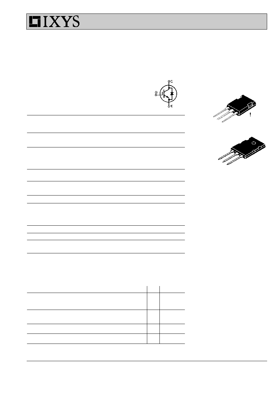
TO-264 AA
G
C
E
G = Gate,
C = Collector,
E = Emitter,
TAB = Collector
Symbol
Test Conditions
Maximum Ratings
V
CES
T
J
= 25
∞
C to 150
∞
C
600
V
V
CGR
T
J
= 25
∞
C to 150
∞
C; R
GE
= 1 M
W
600
V
V
GES
Continuous
±
20
V
V
GEM
Transient
±
30
V
I
C25
T
C
= 25
∞
C, limited by leads
75
A
I
C90
T
C
= 90
∞
C
50
A
I
CM
T
C
= 25
∞
C, 1 ms
200
A
SSOA
V
GE
= 15 V, T
VJ
= 125
∞
C, R
G
= 22
W
I
CM
= 100
A
(RBSOA)
Clamped inductive load, L = 30
m
H
@ 0.8 V
CES
t
SC
V
GE
= 15 V, V
CE
= 360 V, T
J
= 125
∞
C
10
m
s
(SCSOA)
R
G
= 22
W,
non repetitive
P
C
T
C
= 25
∞
C
300
W
T
J
-55 ... +150
∞
C
T
JM
150
∞
C
T
stg
-55 ... +150
∞
C
M
d
Mounting torque
0.9/6
Nm/lb.in.
Weight
10
g
Maximum lead temperature for soldering
300
∞
C
1.6 mm (0.062 in.) from case for 10 s
IGBT with Diode
V
CES
= 600 V
I
C25
= 75 A
V
CE(sat)
= 2.5 V
Short Circuit SOA Capability
Symbol
Test Conditions
Characteristic Values
(T
J
= 25
∞
C, unless otherwise specified)
min.
typ.
max.
BV
CES
I
C
= 3 mA, V
GE
= 0 V
600
V
V
GE(th)
I
C
= 4 mA, V
CE
= V
GE
4
8
V
I
CES
V
CE
= 0.8 ∑ V
CES
T
J
= 25
∞
C
325
m
A
V
GE
= 0 V
T
J
= 125
∞
C
17
mA
I
GES
V
CE
= 0 V, V
GE
=
±
20 V
±
100
nA
V
CE(sat)
I
C
= I
C90
; V
GE
= 15 V,
2.2
2.5
V
Features
∑ International standard package
JEDEC TO-264 AA, and hole-less
TO-247 package for clip mounting
∑ Guaranteed Short Circuit SOA
capability
∑ High frequency IGBT and anti-
parallel FRED in one package
∑ Latest generation HDMOS
TM
process
∑ Low V
CE(sat)
- for minimum on-state conduction
losses
∑ MOS Gate turn-on
- drive simplicity
∑ Fast Recovery
Epitaxial Diode (FRED)
- soft recovery with low I
RM
Applications
∑ AC motor speed control
∑ DC servo and robot drives
∑ DC choppers
∑ Uninterruptible power supplies (UPS)
∑ Switch-mode and resonant-mode
power supplies
Advantages
∑ Space savings (two devices in one
package)
∑ Easy to mount with 1 screw
(isolated mounting screw hole)
∑ Reduces assembly time and cost
97520A (12/98)
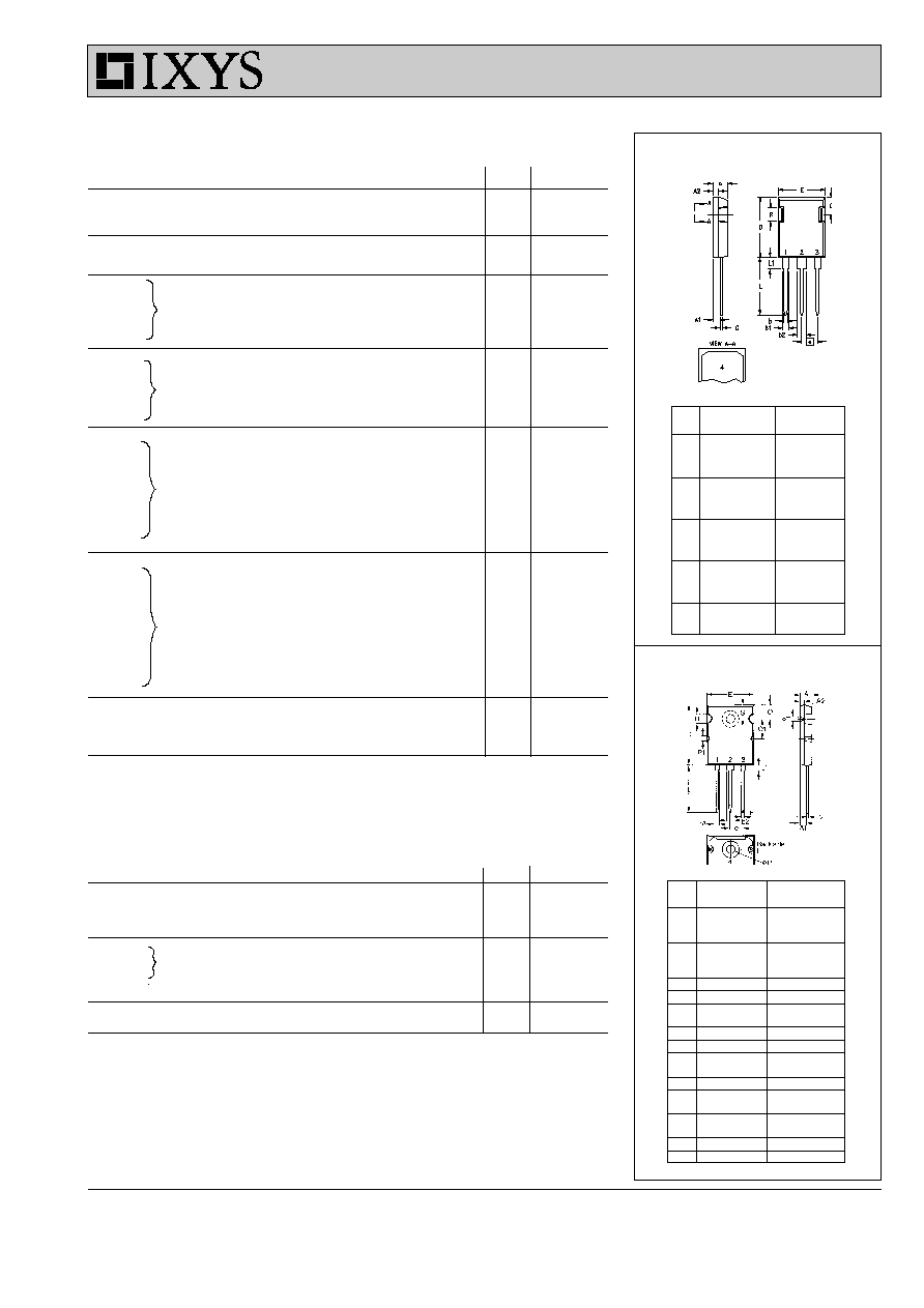
IXSK 50N60BU1
IXSX 50N60BU1
PLUS247
(IXSX)
G
C
E
C (TAB)
(IXSK)
IXYS reserves the right to change limits, test conditions, and dimensions.
2 - 6
© 2000 IXYS All rights reserved
Symbol
Test Conditions
Characteristic Values
(T
J
= 25
∞
C, unless otherwise specified)
min.
typ.
max.
g
fs
I
C
= I
C90
; V
CE
= 10 V,
20
23
S
Pulse test, t
£
300
m
s, duty cycle
£
2 %
I
C(on)
V
GE
= 15 V, V
CE
= 10 V
160
A
C
ies
3850
pF
C
oes
V
CE
= 25 V, V
GE
= 0 V, f = 1 MHz
440
pF
C
res
50
pF
Q
g
167
nC
Q
ge
I
C
= I
C90
, V
GE
= 15 V, V
CE
= 0.5 V
CES
45
nC
Q
gc
88
nC
t
d(on)
70
ns
t
ri
70
ns
t
d(off)
150
300
ns
t
fi
150
300
ns
E
off
3.3
6.0
mJ
t
d(on)
70
ns
t
ri
70
ns
E
on
2.5
mJ
t
d(off)
230
ns
t
fi
230
ns
E
off
4.8
mJ
R
thJC
0.42 K/W
R
thCK
0.15
K/W
Reverse Diode (FRED)
Characteristic Values
(T
J
= 25
∞
C, unless otherwise specified)
Symbol
Test Conditions
min.
typ.
max.
V
F
I
F
= I
C90
, V
GE
= 0 V,
1.8
V
Pulse test, t
£
300
m
s, duty cycle d
£
2 %
I
RM
I
F
= I
C90
, V
GE
= 0 V, -di
F
/dt = 480 A/
m
s
19
33
A
t
rr
V
R
= 360 V
T
J
= 125
∞
C
175
ns
I
F
= 1 A; -di/dt = 200 A/
m
s; V
R
= 30 V
T
J
= 25
∞
C
35
50
ns
R
thJC
0.75 K/W
Inductive load, T
J
= 25
∞
C
I
C
= I
C90
, V
GE
= 15 V, L = 100
m
H,
V
CE
= 0.8 V
CES
, R
G
= 2.7
W
Remarks: Switching times may increase
for V
CE
(Clamp) > 0.8 ∑ V
CES
, higher T
J
or
increased R
G
Inductive load, T
J
= 125
∞
C
I
C
= I
C90
, V
GE
= 15 V, L = 100
m
H
V
CE
= 0.8 V
CES
, R
G
= 2.7
W
Remarks: Switching times may increase
for V
CE
(Clamp) > 0.8 ∑ V
CES
, higher T
J
or
increased R
G
PLUS247
TM
(IXSX)
Dim.
Millimeter
Inches
Min.
Max.
Min. Max.
A
4.83
5.21
.190 .205
A
1
2.29
2.54
.090 .100
A
2
1.91
2.16
.075 .085
b
1.14
1.40
.045 .055
b
1
1.91
2.13
.075 .084
b
2
2.92
3.12
.115 .123
C
0.61
0.80
.024 .031
D
20.80
21.34
.819 .840
E
15.75
16.13
.620 .635
e 5.45 BSC
.215 BSC
L
19.81
20.32
.780 .800
L1
3.81
4.32
.150 .170
Q
5.59
6.20
.220 .244
R
4.32
4.83
.170 .190
Millimeter
Inches
Min.
Max.
Min.
Max.
A
4.82
5.13
.190
.202
A1
2.54
2.89
.100
.114
A2
2.00
2.10
.079
.083
b
1.12
1.42
.044
.056
b1
2.39
2.69
.094
.106
b2
2.90
3.09
.114
.122
c
0.53
0.83
.021
.033
D
25.91
26.16
1.020
1.030
E
19.81
19.96
.780
.786
e
5.46 BSC
.215 BSC
J
0.00
0.25
.000
.010
K
0.00
0.25
.000
.010
L
20.32
20.83
.800
.820
L1
2.29
2.59
.090
.102
P
3.17
3.66
.125
.144
Q
6.07
6.27
.239
.247
Q1
8.38
8.69
.330
.342
R
3.81
4.32
.150
.170
R1
1.78
2.29
.070
.090
S
6.04
6.30
.238
.248
T
1.57
1.83
.062
.072
Dim.
TO-264 AA Outline
IXSK 50N60BU1
IXSX 50N60BU1
IXYS MOSFETS and IGBTs are covered by one or more of the following U.S. patents:
4,835,592
4,881,106
5,017,508
5,049,961
5,187,117
5,486,715
4,850,072
4,931,844
5,034,796
5,063,307
5,237,481
5,381,025

3 - 6
© 2000 IXYS All rights reserved
V
GE
- Volts
4
6
8
10
12
14
16
I
C
- A
m
p
e
res
0
20
40
60
80
100
V
CE
-Volts
0
5
10
15
20
25
30
35
40
C
a
pac
i
t
a
nc
e -
pF
10
100
1000
10000
T
J
- Degrees C
25
50
75
100
125
150
V
C
E
(
sat
)
-
N
o
r
m
a
liz
e
d
0.4
0.6
0.8
1.0
1.2
1.4
1.6
V
CE
- Volts
0
2
4
6
8
10
I
C
-
A
m
p
e
r
e
s
0
20
40
60
80
100
V
CE
- Volts
0
4
8
12
16
20
I
C
-
A
m
p
e
re
s
0
40
80
120
160
13V
11V
9V
V
CE
= 10V
T
J
= 25∞C
V
GE
= 15V
T
J
= 25∞C
I
C
= 25A
I
C
= 50A
I
C
= 100A
T
J
=
125∞C
C
rss
f = 1Mhz
9V
V
GE
= 15V
T
J
= 25∞C
V
CE
- Volts
0
2
4
6
8
10
I
C
- A
m
p
e
re
s
0
20
40
60
80
100
T
J
= 125∞C
C
iss
C
oss
7V
9V
11V
7V
13V
V
GE
= 15V
13V
11V
V
GE
= 15V
IXSK 50N60BU1
IXSX 50N60BU1
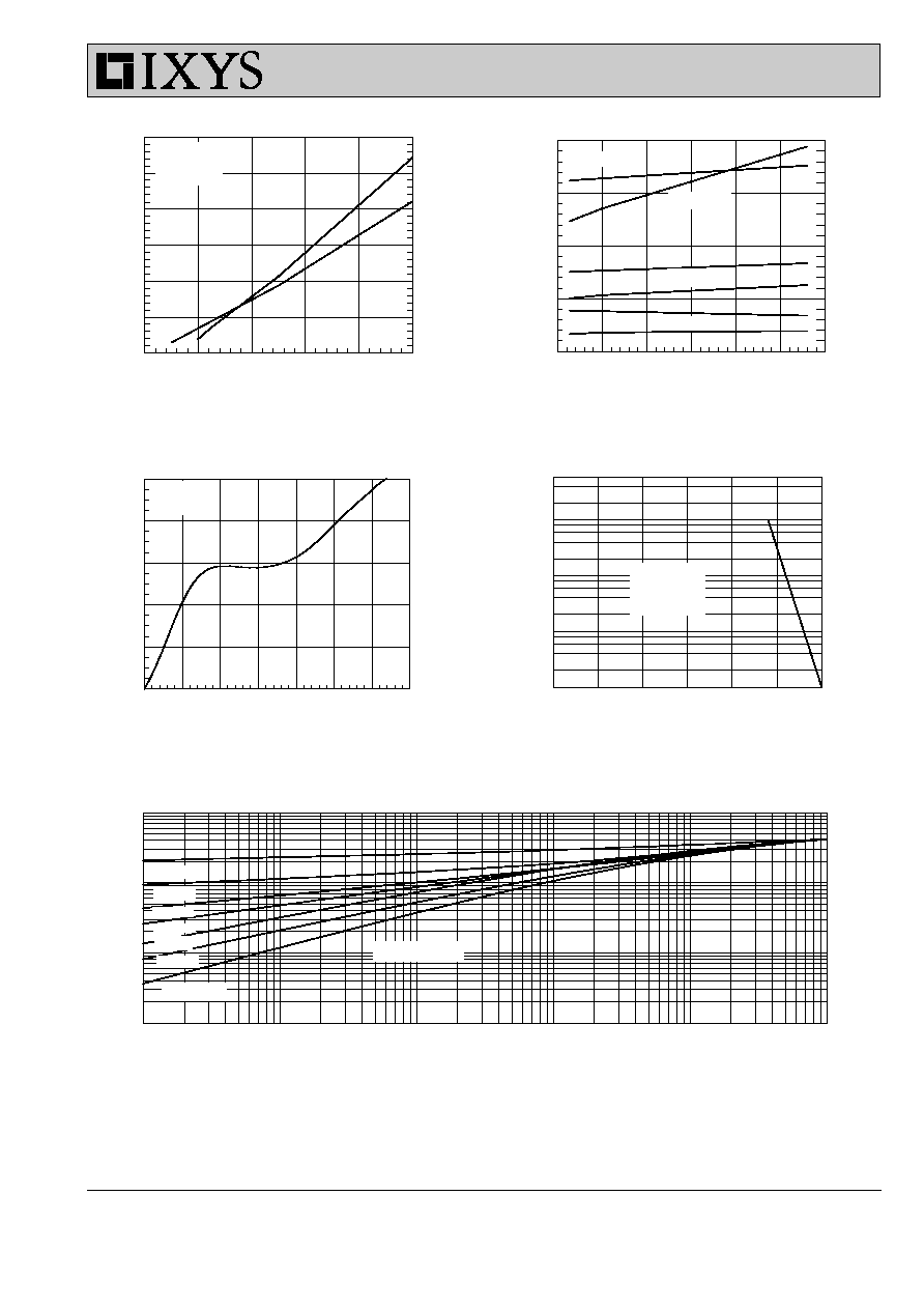
Figure 1. Saturation Voltage Characteristics
Figure 2. Extended Output Characteristics
Figure 3. Saturation Voltage Characteristics
Figure 4. Temperature Dependence of V
CE(sat)
Figure 5. Admittance Curves
Figure 6. Capacitance Curves
4 - 6
© 2000 IXYS All rights reserved
Pulse Width - Seconds
0.00001
0.0001
0.001
0.01
0.1
1
Z
th
JC
(K
/
W
)
0.001
0.01
0.1
1
D=0.02
V
CE
- Volts
0
100
200
300
400
500
600
I
C
- A
m
per
e
s
0.1
1
10
100
Q
g
- nanocoulombs
0
25
50
75
100
125
150
175
0
4
8
12
16
20
R
G
- Ohms
0
10
20
30
40
50
60
E
(
O
FF)
-
mill
ijou
l
es
0
5
10
15
20
E
(ON
)
-
milli
joul
es
0
1
2
3
4
I
C
- Amperes
0
20
40
60
80
100
E
(
O
FF)
-
m
i
lli
Joules
0
4
8
12
16
20
24
E
(O
N
)
-
mill
ijo
u
les
0.0
0.5
1.0
1.5
2.0
2.5
3.0
V
CE
= 250V
I
C
=50A
E
(ON)
E
(OFF)
E
(ON)
E
(OFF)
T
J
= 125∞C
R
G
= 6.2
dV/dt < 5V/ns
D=0.1
D=0.05
Single pulse
D = Duty Cycle
T
J
= 125∞C
R
G
= 10
600
E
(OFF)
E
(OFF)
D=0.2
D=0.5
D=0.01
I
C
=25A
T
J
= 125∞C
I
C
= 100A
I
C
= 50A
E
(ON)
E
(ON)
IXSK 50N60BU1
IXSX 50N60BU1
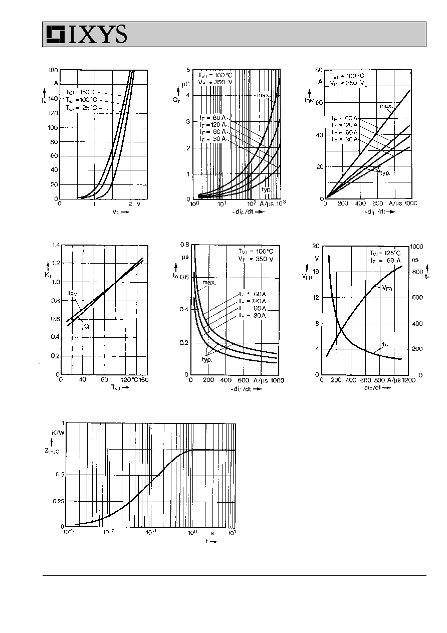
Figure 9. Gate Charge
Figure 10. Turn-off Safe Operating Area
Figure 11. Transient Thermal Resistance
Figure 7. Dependence of E
ON
and E
OFF
on I
C
.
Figure 8. Dependence of E
ON
and E
OFF
on
R
G
.
5 - 6
© 2000 IXYS All rights reserved
IXSK 50N60BU1
IXSX 50N60BU1
Fig. 12 Forward current
Fig. 13 Recovery charge versus -di
F
/dt.
Fig. 14 Peak reverse current versus
versus voltage drop.
-di
F
/dt.
Fig. 15. Dynamic parameters versus
Fig. 16 Recovery time versus -di
F
/dt.
Fig. 17 Peak forward voltage vs. di
F
/dt.
junction temperature.
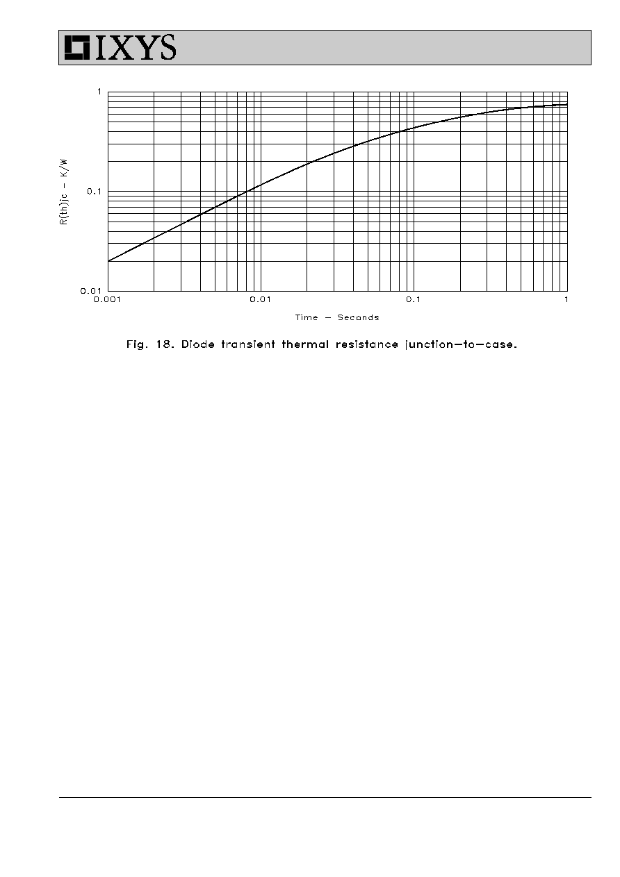
Fig. 18 Transient thermal impedance junction to case.
6 - 6
© 2000 IXYS All rights reserved
IXSK 50N60BU1
IXSX 50N60BU1