© 2002 IXYS All rights reserved
Symbol
Test Conditions
Maximum Ratings
V
CES
T
J
= 25
∞
C to 150
∞
C
1200
V
V
CGR
T
J
= 25
∞
C to 150
∞
C; R
GE
= 1 M
1200
V
V
GES
Continuous
±
20
V
V
GEM
Transient
±
30
V
I
C25
T
C
= 25
∞
C
70
A
I
C90
T
C
= 90
∞
C
30
A
I
CM
T
C
= 25
∞
C, 1 ms
140
A
SSOA
V
GE
= 15 V, T
VJ
= 125
∞
C, R
G
= 22
I
CM
= 90
A
(RBSOA)
Clamped inductive load, L = 30
µ
H
@ 0.8 V
CES
t
SC
V
GE
= 15 V, V
CE
= 720 V, T
J
= 125
∞
C
10
µ
s
(SCSOA)
R
G
= 22
,
non repetitive
P
C
T
C
= 25
∞
C
IGBT
250
W
Diode
150
W
T
J
-55 ... +150
∞
C
T
JM
150
∞
C
T
stg
-55 ... +150
∞
C
V
ISOL
50/60 Hz, RMS
t = 1 min leads-to housing
2500
V~
Maximum lead temperature for soldering
300
∞
C
1.6 mm (0.062 in.) from case for 10 s
Weight
5
g
V
CES
= 1200 V
I
C25
= 70 A
V
CE(sat)
= 3.6 V
t
fi(typ)
= 180 ns
Symbol
Test Conditions
Characteristic Values
(T
J
= 25
∞
C, unless otherwise specified)
min.
typ.
max.
BV
CES
I
C
= 3 mA, V
GE
= 0 V
1200
V
V
GE(th)
I
C
=
250
µ
A,
V
CE
= V
GE
3
6
V
I
CES
V
CE
= 0.8 ∑ V
CES
T
J
= 25
∞
C
1 mA
V
GE
= 0 V
T
J
= 150
∞
C
3 mA
I
GES
V
CE
= 0 V, V
GE
=
±
20 V
±
100
nA
V
CE(sat)
I
C
=
I
T,
V
GE
= 15 V
3.6
V
98741A (01/02)
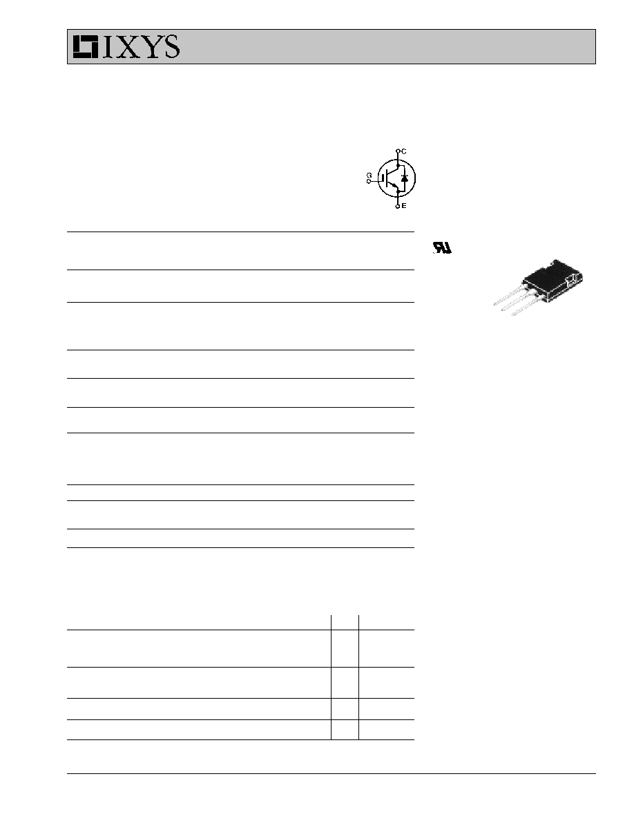
IGBT with Diode
ISOPLUS 247
TM
(Electrically Isolated Backside)
Short Circuit SOA Capability
IXSR 35N120BD1
Features
DCB Isolated mounting tab
Meets TO-247AD package outline
High current handling capability
Latest generation HDMOS
TM
process
MOS Gate turn-on
- drive simplicity
Applications
Uninterruptible power supplies (UPS)
Switched-mode and resonant-mode
power supplies
AC motor speed control
DC servo and robot drives
DC choppers
Advantages
Easy assembly
High power density
ISOPLUS 247
TM
G
C
Isolated backside*
E 153432
E
G = Gate,
C = Collector,
E = Emitter
* Patent pending
Device must be heatsunk for high temperature measurements to avoid thermal runaway.
IXYS reserves the right to change limits, test conditions and dimensions
IXYS reserves the right to change limits, test conditions, and dimensions.
IXYS MOSFETS and IGBTs are covered by one or more of the following U.S. patents:
4,835,592
4,881,106
5,017,508
5,049,961
5,187,117
5,486,715
6,306,728B1
4,850,072
4,931,844
5,034,796
5,063,307
5,237,481
5,381,025
IXSR 35N120BD1
Symbol
Test Conditions
Characteristic Values
(T
J
= 25
∞
C, unless otherwise specified)
min.
typ.
max.
g
fs
I
C
=
I
T
; V
CE
= 10 V,
16
23
S
Pulse test, t
300
µ
s, duty cycle
2 %
C
iss
3600
pF
C
oss
V
GS
= 0 V, V
DS
= 25 V, f = 1 MHz
315
pF
C
rss
75
pF
Q
g
120
nC
Q
ge
I
C
=
I
T,
V
GE
= 15 V, V
CE
= 0.5 V
CES
33
nC
Q
gc
49
nC
t
d(on)
36
ns
t
ri
27
ns
t
d(off)
160
300
ns
t
fi
180
300
ns
E
off
5
9 mJ
t
d(on)
38
ns
t
ri
29
ns
E
on
6
mJ
t
d(off)
240
ns
t
fi
340
ns
E
off
9
mJ
R
thJC
0.5 K/W
R
thCK
0.15
K/W
Reverse Diode (FRED)
Characteristic Values
(T
J
= 25
∞
C, unless otherwise specified)
Symbol
Test Conditions
min.
typ.
max.
V
F
I
F
=
I
T,
V
GE
= 0 V,
2.75
V
Pulse test, t
300
µ
s, duty cycle d
2 %
1.85
I
RM
I
F
=
I
T,
V
GE
= 0 V, -di
F
/dt = 100 A/
µ
s
7 14.3
A
t
rr
V
R
= 100 V
I
F
= 1 A; -di/dt = 200 A/
µ
s; V
R
= 30 V
40
ns
R
thJC
0.83 K/W
Inductive load, T
J
= 25
∞∞
∞∞
∞
C
I
C
=
I
T,
V
GE
= 15 V, L = 100
µ
H,
V
CE
= 0.8 V
CES
, R
G
= 2.7
Remarks: Switching times may increase
for V
CE
(Clamp) > 0.8 ∑ V
CES
, higher T
J
or
increased R
G
Inductive load, T
J
= 125
∞∞
∞∞
∞
C
I
C
=
I
T,
V
GE
= 15 V, L = 100
µ
H
V
CE
= 0.8 V
CES
, R
G
= 2.7
Remarks: Switching times may increase
for V
CE
(Clamp) > 0.8 ∑ V
CES
, higher T
J
or
increased R
G
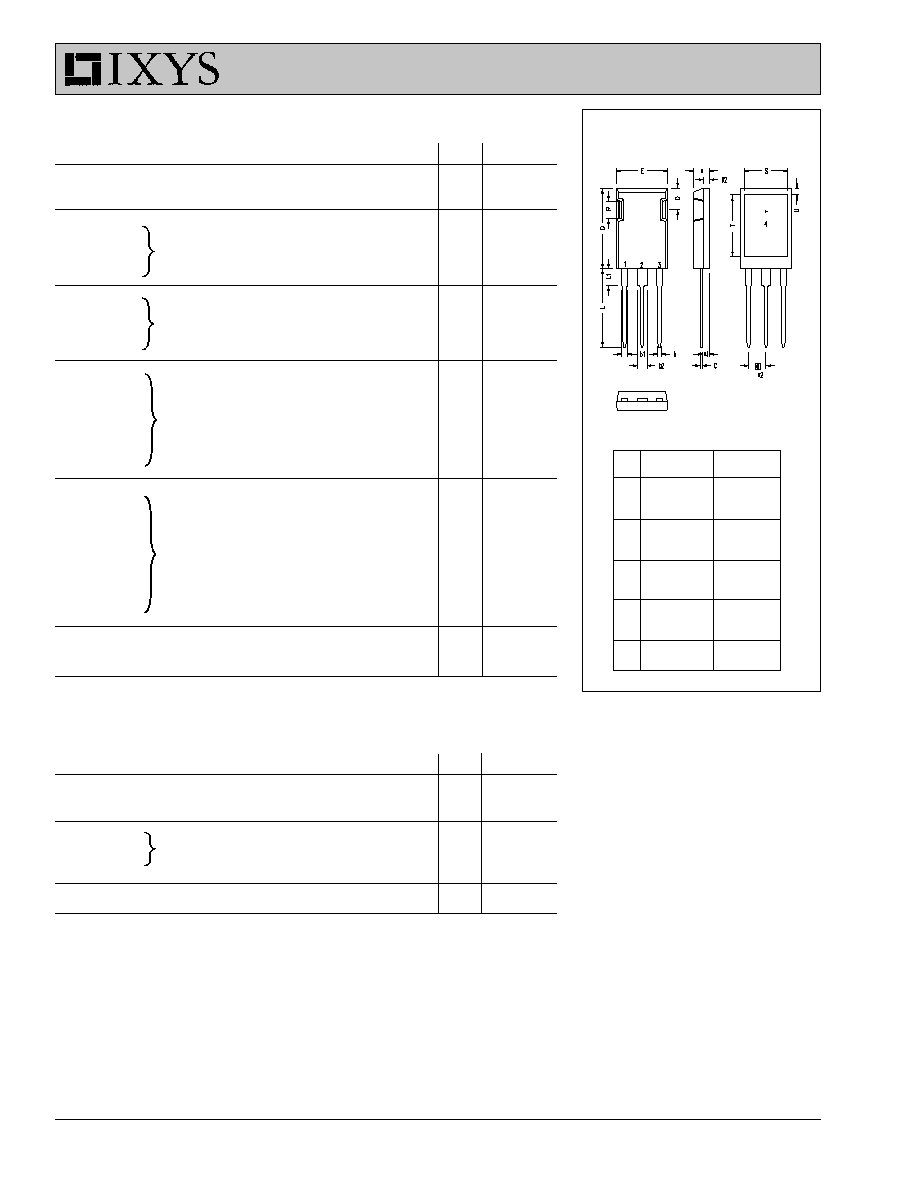
ISOPLUS 247 OUTLINE
Dim.
Millimeter
Inches
Min.
Max.
Min. Max.
A
4.83
5.21
.190 .205
A
1
2.29
2.54
.090 .100
A
2
1.91
2.16
.075 .085
b
1.14
1.40
.045 .055
b
1
1.91
2.13
.075 .084
b
2
2.92
3.12
.115 .123
C
0.61
0.80
.024 .031
D
20.80
21.34
.819 .840
E
15.75
16.13
.620 .635
e 5.45 BSC
.215 BSC
L
19.81
20.32
.780 .800
L1
3.81
4.32
.150 .170
Q
5.59
6.20
.220 .244
R
4.32
4.83
.170 .190
1 Gate, 2 Drain (Collector)
3 Source (Emitter)
4 no connection
Note: 1. I
T
= 35A