 | ÐлекÑÑоннÑй компоненÑ: IXTA8N50P | СкаÑаÑÑ:  PDF PDF  ZIP ZIP |
DS99321A(IXTA-IXTP8N50P)
© 2005 IXYS All rights reserved
Symbol
Test Conditions
Maximum Ratings
V
DSS
T
J
= 25
°C to 150°C
500
V
V
DGR
T
J
= 25
°C to 150°C; R
GS
= 1 M
500
V
V
GS
Continuous
±20
V
V
GSM
Transient ±30 V
I
D25
T
C
= 25
°C
8
A
I
DM
T
C
= 25
°C, pulse width limited by T
JM
14
A
I
AR
T
C
= 25
°C
8
A
E
AR
T
C
= 25
°C
17
mJ
E
AS
T
C
= 25
°C
300
mJ
dv/dt
I
S
I
DM
, di/dt
100 A/µs, V
DD
V
DSS
,
10
V/ns
T
J
150°C, R
G
= 10
P
D
T
C
= 25
°C
150
W
T
J
-55 ... +150
°C
T
JM
150
°C
T
stg
-55 ... +150
°C
T
L
1.6 mm (0.062 in.) from case for 10 s
300
°C
Maximum tab temperature for soldering
260
°C
TO-263 package for 10s
M
d
Mounting torque
(TO-220)
1.13/10 Nm/lb.in.
Weight
TO-220
4
g
TO-263
3
g
G = Gate
D = Drain
S = Source
TAB = Drain
DS99321(08/05)
Symbol
Test Conditions
Characteristic Values
(T
J
= 25
°C unless otherwise specified)
Min. Typ.
Max.
V
DSS
V
GS
= 0 V, I
D
= 250
µA
500
V
V
GS(th)
V
DS
= V
GS
, I
D
= 250
µA
2.5
5.0
V
I
GSS
V
GS
=
±20 V
DC
, V
DS
= 0
±100
nA
I
DSS
V
DS
= V
DSS
5
µA
V
GS
= 0 V
T
J
= 125
°C
50
µA
R
DS(on)
V
GS
= 10 V, I
D
= 0.5 I
D25
0.8
Pulse test, t
300 µs, duty cycle d 2 %
PolarHV
TM
Power MOSFET
Advance Technical Information
N-Channel Enhancement Mode
Avalanche Energy Rated
Features
International standard packages
Unclamped Inductive Switching (UIS)
rated
Low package inductance
- easy to drive and to protect
Advantages
Easy to mount
Space savings
High power density
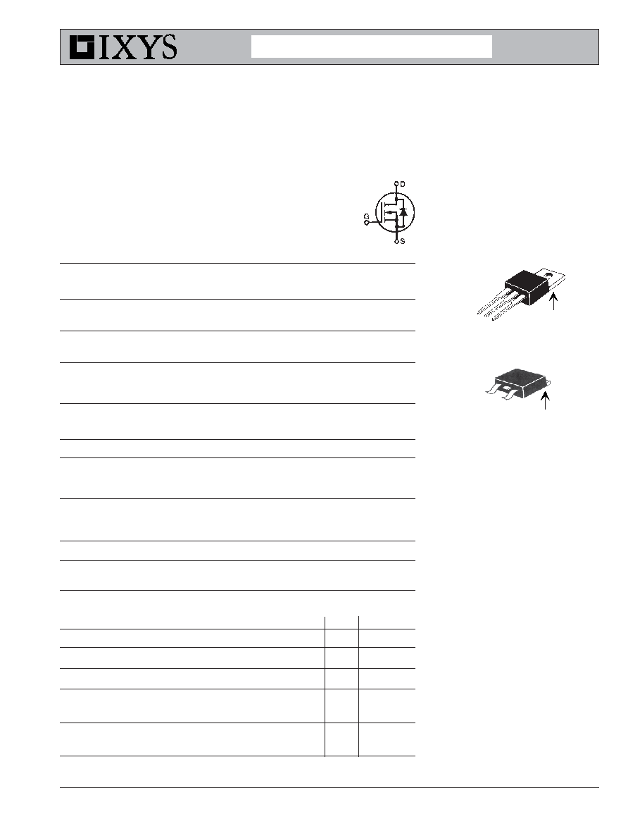
TO-263 (IXTA)
TO-220 (IXTP)
D
(TAB)
G
S
G
S
(TAB)
IXTA 8N50P
IXTP 8N50P
V
DSS
= 500 V
I
D25
= 8 A
R
DS(on)
= 0.8
IXYS reserves the right to change limits, test conditions, and dimensions.
IXTA 8N50P
IXTP 8N50P
Symbol
Test Conditions Characteristic Values
(T
J
= 25
°C unless otherwise specified)
Min.
Typ.
Max.
g
fs
V
DS
= 10 V; I
D
= 0.5 I
D25
, pulse test
5
8
S
C
iss
1050
pF
C
oss
V
GS
= 0 V, V
DS
= 25 V, f = 1 MHz
120
pF
C
rss
12
pF
t
d(on)
20
n s
t
r
V
GS
= 10 V, V
DS
= 0.5 V
DSS
, I
D
= I
D25
25
n s
t
d(off)
R
G
= 10
(External)
60
n s
t
f
18
n s
Q
g(on)
20
nC
Q
gs
V
GS
= 10 V, V
DS
= 0.5 V
DSS
, I
D
= 0.5 I
D25
7
nC
Q
gd
7
nC
R
thJC
0.83 K/W
R
thCK
(TO-220)
0.25
K/W
Source-Drain Diode Characteristic Values
(T
J
= 25
°C, unless otherwise specified)
Symbol
Test Conditions
Min.
typ.
Max.
I
S
V
GS
= 0 V
8
A
I
SM
Repetitive
14
A
V
SD
I
F
= I
S
, V
GS
= 0 V,
1.5
V
Pulse test, t
300 µs, duty cycle d 2 %
t
rr
I
F
= 3 A, V
GS
=0V, V
R
=100V
400
n s
-di/dt = 100 A/
µs
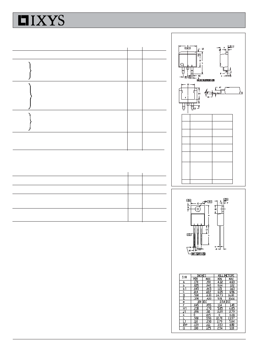
Pins: 1 - Gate
2 - Drain
3 - Source
4 - Drain
TO-220 (IXTP) Outline
Dim.
Millimeter
Inches
Min.
Max.
Min.
Max.
A
4.06
4.83
.160
.190
A1
2.03
2.79
.080
.110
b
0.51
0.99
.020
.039
b2
1.14
1.40
.045
.055
c
0.46
0.74
.018
.029
c2
1.14
1.40
.045
.055
D
8.64
9.65
.340
.380
D1
7.11
8.13
.280
.320
E
9.65
10.29
.380
.405
E1
6.86
8.13
.270
.320
e
2.54
BSC
.100
BSC
L
14.61
15.88
.575
.625
L1
2.29
2.79
.090
.110
L2
1.02
1.40
.040
.055
L3
1.27
1.78
.050
.070
L4
0
0.38
0
.015
R
0.46
0.74
.018
.029
TO-263 (IXTA) Outline
Pins: 1 - Gate 3 - Source
2, 4 - Drain
IXYS MOSFETs and IGBTs are covered by
4,835,592
4,931,844
5,049,961
5,237,481
6,162,665
6,404,065 B1
6,683,344
6,727,585
one or moreof the following U.S. patents:
4,850,072
5,017,508
5,063,307
5,381,025
6,259,123 B1
6,534,343
6,710,405B2
6,759,692
4,881,106
5,034,796
5,187,117
5,486,715
6,306,728 B1
6,583,505
6,710,463
© 2005 IXYS All rights reserved
IXTA 8N50P
IXTP 8N50P
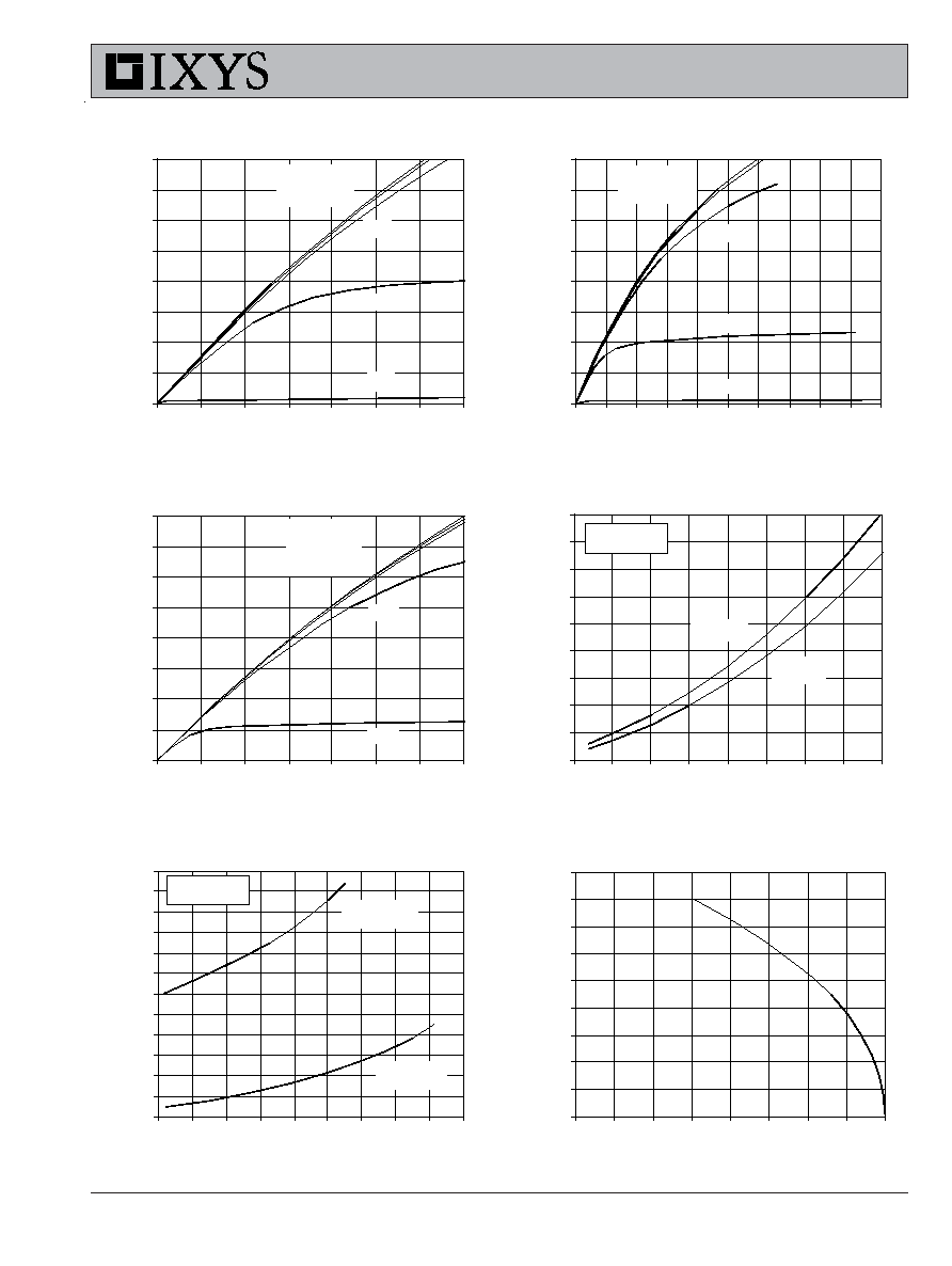
Fig. 2. Extended Output Characteristics
@ 25
º
C
0
2
4
6
8
10
12
14
16
0
3
6
9
12
15
18
21
24
27
30
V
D S
- Volts
I
D
-
A
m
per
es
V
GS
= 10V
8V
5V
7V
6V
Fig. 3. Output Characteristics
@ 125
º
C
0
1
2
3
4
5
6
7
8
0
2
4
6
8
10
12
14
V
D S
- Volts
I
D
-
A
m
per
es
V
GS
= 10V
8V
7V
5V
6V
Fig. 1. Output Characteristics
@ 25
º
C
0
1
2
3
4
5
6
7
8
0
1
2
3
4
5
6
7
V
D S
- Volts
I
D
-
A
m
per
es
V
GS
= 10V
8V
7V
6V
5V
Fig. 4. R
DS(on
)
Norm alized to 0.5 I
D25
Value vs. Junction Tem perature
0.4
0.7
1
1.3
1.6
1.9
2.2
2.5
2.8
3.1
-50
-25
0
25
50
75
100
125
150
T
J
- Degrees Centigrade
R
D
S
(
o n )
-
N
o
rm
a
l
i
z
e
d
I
D
= 8A
I
D
= 4A
V
GS
= 10V
Fig. 6. Drain Current vs. Case
Tem perature
0
1
2
3
4
5
6
7
8
9
-50
-25
0
25
50
75
100
125
150
T
C
- Degrees Centigrade
I
D
-
A
m
per
es
Fig. 5. R
DS(on)
Norm alized to
0.5 I
D25
Value vs. I
D
0.8
1
1.2
1.4
1.6
1.8
2
2.2
2.4
2.6
2.8
3
3.2
0
2
4
6
8
10
12
14
16
18
I
D
- Amperes
R
D
S
(
o n )
-
N
o
rm
a
l
i
z
e
d
T
J
= 125
C
T
J
= 25
C
V
GS
= 10V
IXYS reserves the right to change limits, test conditions, and dimensions.
IXTA 8N50P
IXTP 8N50P
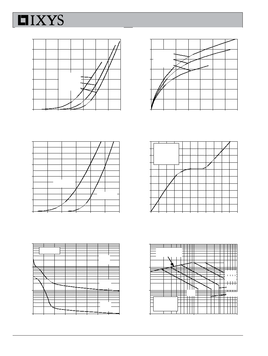
Fig. 11. Capacitance
10
100
1000
10000
0
5
10
15
20
25
30
35
40
V
D S
- Volts
C
a
pac
i
t
anc
e
-
pic
o
F
a
r
ads
Ciss
Coss
Crss
f = 1MHz
Fig. 10. Gate Charge
0
1
2
3
4
5
6
7
8
9
10
0
2
4
6
8
10
12
14
16
18
20
22
Q
G
- nanoCoulombs
V
G S
- V
o
l
t
s
V
DS
= 250V
I
D
= 4A
I
G
= 10mA
Fig. 7. Input Adm ittance
0
2
4
6
8
10
12
14
3.5
4
4.5
5
5.5
6
6.5
7
V
G S
- Volts
I
D
-
A
m
p
e
r
e
s
T
J
= 125
C
25
C
-40
C
Fig. 8. Transconductance
0
2
4
6
8
10
12
14
0
2
4
6
8
10
12
14
I
D
- Amperes
g
f s
- S
i
e
m
e
n
s
T
J
= -40
C
25
C
125
C
Fig. 9. Source Current vs.
Source-To-Drain Voltage
0
4
8
12
16
20
24
0.4
0.5
0.6
0.7
0.8
0.9
1
V
S D
- Volts
I
S
- A
m
p
e
r
e
s
T
J
= 125
C
T
J
= 25
C
Fig. 12. Forw ard-Bias
Safe Operating Area
0.1
1
10
100
10
100
1000
V
D S
- Volts
I
D
- A
m
p
e
r
e
s
100µs
1ms
DC
T
J
= 150C
T
C
= 25C
R
DS(on)
Limit
10ms
25µs
© 2005 IXYS All rights reserved
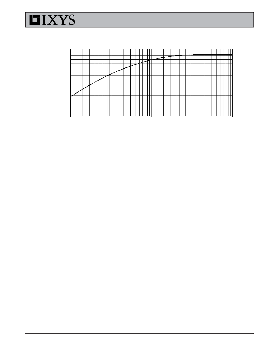
Fig. 13. Maxim um Transient Thermal Resistance
0.10
1.00
0.001
0.01
0.1
1
10
Pulse Width - Seconds
R
( t h ) J
C
-
C /
W
IXTA 8N50P
IXTP 8N50P