 | –≠–ª–µ–∫—Ç—Ä–æ–Ω–Ω—ã–π –∫–æ–º–ø–æ–Ω–µ–Ω—Ç: IXTH75N15 | –°–∫–∞—á–∞—Ç—å:  PDF PDF  ZIP ZIP |
© 2003 IXYS All rights reserved
Symbol
Test Conditions
Maximum Ratings
V
DSS
T
J
= 25
∞
C to 150
∞
C
150
V
V
DGR
T
J
= 25
∞
C to 150
∞
C; R
GS
= 1 M
150
V
V
GS
Continuous
±
20
V
V
GSM
Transient
±
30
V
I
D25
T
C
= 25
∞
C
75
A
I
DM
T
C
= 25
∞
C, pulse width limited by T
JM
300
A
I
AR
T
C
= 25
∞
C
75
A
E
AR
T
C
= 25
∞
C
60
mJ
E
AS
T
C
= 25
∞
C
1.5
J
dv/dt
I
S
I
DM
, di/dt
100 A/
µ
s, V
DD
V
DSS
,
5
V/ns
T
J
150
∞
C, R
G
= 2
P
D
T
C
= 25
∞
C
330
W
T
J
-55 ... +150
∞
C
T
JM
150
∞
C
T
stg
-55 ... +150
∞
C
T
L
1.6 mm (0.062 in.) from case for 10 s
300
∞
C
M
d
Mounting torque
1.13/10 Nm/lb.in.
Weight
TO-247 AD
6
g
TO-268
4
g
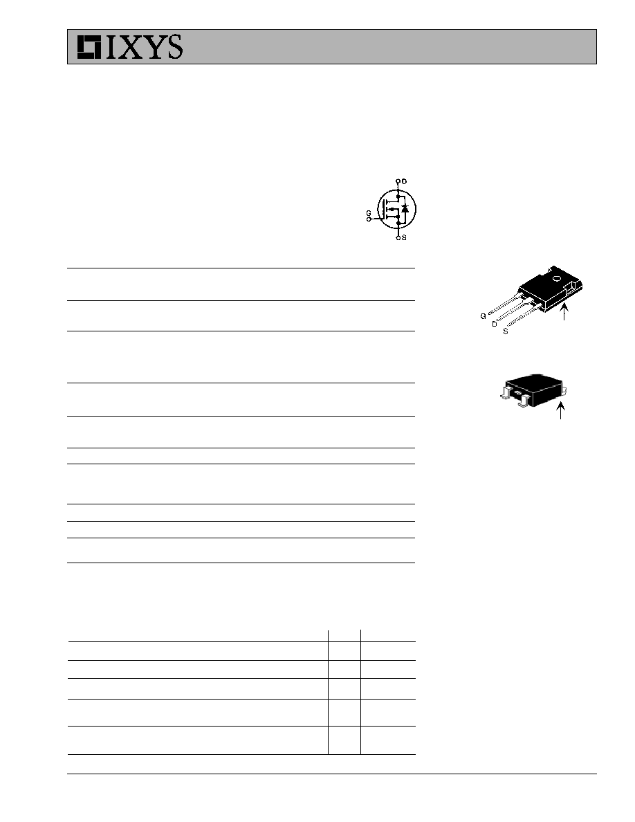
TO-247 AD (IXTH)
G = Gate
D = Drain
S = Source
TAB = Drain
(TAB)
DS98948A(02/03)
Symbol
Test Conditions
Characteristic Values
(T
J
= 25
∞
C, unless otherwise specified)
Min. Typ.
Max.
V
DSS
V
GS
= 0 V, I
D
=
250 µ
A
150
V
V
GS(th)
V
DS
= V
GS
, I
D
=
250µ
A
2.0
4.0
V
I
GSS
V
GS
=
±
20 V
DC
, V
DS
= 0
±
100
nA
I
DSS
V
DS
= V
DSS
T
J
= 25
∞
C
25
µ
A
V
GS
= 0 V
T
J
= 125
∞
C
250
µ
A
R
DS(on)
V
GS
= 10 V, I
D
= 0.5 I
D25
23
m
Pulse test, t
300
µ
s, duty cycle d
2 %
TO-268
(IXTT)
Case Style
(TAB)
G
S
High Current
Power MOSFET
IXTH 75N15
V
DSS
= 150 V
IXTT 75N15
I
D25
= 75 A
R
DS(on)
= 23
m
N-Channel Enhancement Mode
Features
International standard packages
Low R
DS (on)
HDMOS
TM
process
Rugged polysilicon gate cell structure
Unclamped Inductive Switching (UIS)
rated
Low package inductance
- easy to drive and to protect
Advantages
Easy to mount
Space savings
High power density
Preliminary Data Sheet

IXYS reserves the right to change limits, test conditions, and dimensions.
IXYS MOSFETs and IGBTs are covered by one or more of the following U.S. patents:
4,835,592
4,881,106
5,017,508
5,049,961
5,187,117
5,486,715
6,306,728B1
4,850,072
4,931,844
5,034,796
5,063,307
5,237,481
5,381,025
IXTH 75N15
IXTT 75N15
Symbol
Test Conditions
Characteristic Values
(T
J
= 25
∞
C, unless otherwise specified)
Min.
Typ. Max.
g
fs
V
DS
= 10 V; I
D
= 0.5 I
D25
, pulse test
34
45
S
C
iss
3950
pF
C
oss
V
GS
= 0 V, V
DS
= 25 V, f = 1 MHz
1100
pF
C
rss
420
pF
t
d(on)
24
ns
t
r
V
GS
= 10 V, V
DS
= 0.5 V
DSS
, I
D
= 0.5 I
D25
33
ns
t
d(off)
R
G
= 2
(External)
70
ns
t
f
17
ns
Q
g(on)
180
nC
Q
gs
V
GS
= 10 V, V
DS
= 0.5 V
DSS
, I
D
= 0.5 I
D25
33
nC
Q
gd
75
nC
R
thJC
0.35
K/W
R
thCK
(TO-247)
0.21
K/W
Source-Drain Diode
Characteristic Values
(T
J
= 25
∞
C, unless otherwise specified)
Symbol
Test Conditions
min.
typ.
max.
I
S
V
GS
= 0 V
75
A
I
SM
Repetitive
300
A
V
SD
I
F
= I
S
, V
GS
= 0 V,
1.5
V
Pulse test, t
300
µ
s, duty cycle d
2 %
Dim.
Millimeter
Inches
Min.
Max.
Min. Max.
A
4.7
5.3
.185
.209
A
1
2.2
2.54
.087
.102
A
2
2.2
2.6
.059
.098
b
1.0
1.4
.040
.055
b
1
1.65
2.13
.065
.084
b
2
2.87
3.12
.113
.123
C
.4
.8
.016
.031
D
20.80
21.46
.819
.845
E
15.75
16.26
.610
.640
e
5.20
5.72
0.205 0.225
L
19.81
20.32
.780
.800
L1
4.50
.177
P
3.55
3.65
.140
.144
Q
5.89
6.40
0.232 0.252
R
4.32
5.49
.170
.216
S
6.15 BSC
242 BSC
TO-247 AD Outline
Terminals: 1 - Gate
2 - Drain
3 - Source
Tab - Drain
1 2 3
TO-268 Outline
Terminals: 1 - Gate
2 - Drain
3 - Source
Tab - Drain
Min Recommended Footprint
T
rr
I
F
= 25A
-di/dt = 100 A/
µ
s
V
R
= 100V
Q
RM
250
2.0
ns
µ
C
© 2003 IXYS All rights reserved
IXTH 75N15
IXTT 75N15
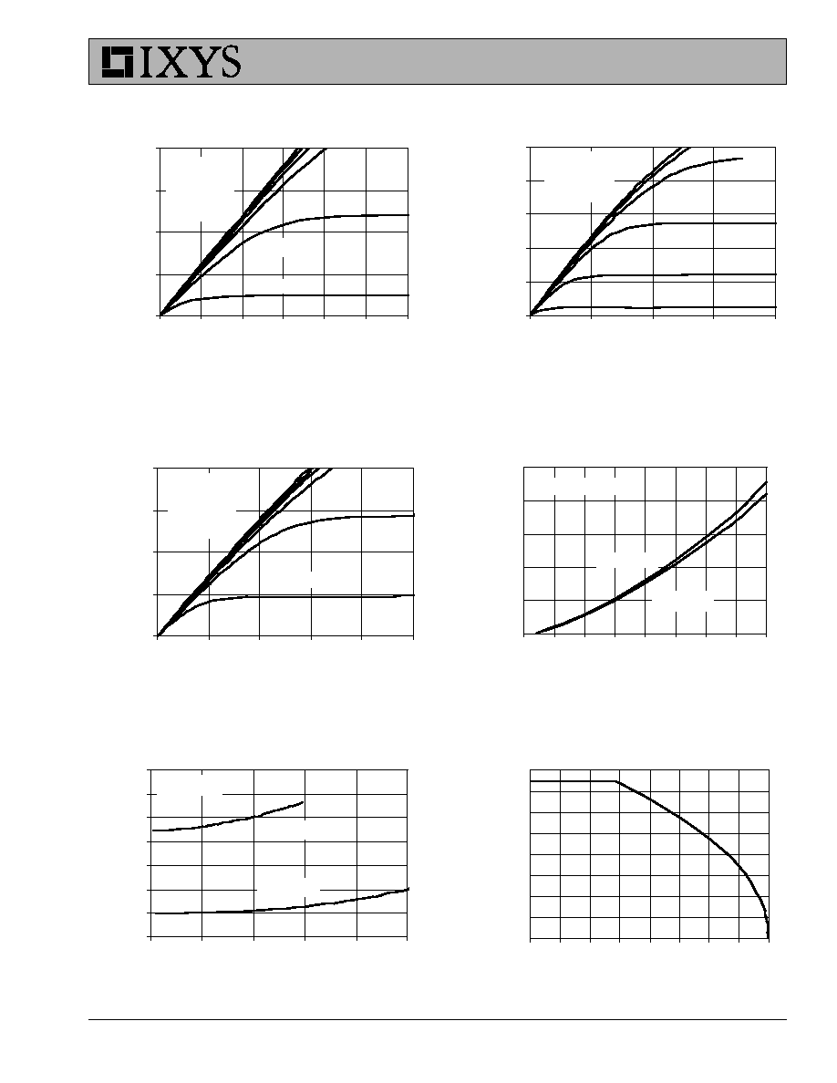
Fig. 6. Drain Current vs. Case
Temperature
0
10
20
30
40
50
60
70
80
-50 -25
0
25
50
75 100 125 150
T
C
- Degrees Centigrade
I
D
- A
m
p
e
r
e
s
Fig. 5. R
DS(on)
Normalized to I
D25
Value vs. I
D
0.8
1
1.2
1.4
1.6
1.8
2
2.2
0
40
80
120
160
200
I
D
- Am peres
R
DS
(
o
n
)
- N
o
r
m
a
l
i
z
e
d
T
J
= 125
∫
C
T
J
= 25
∫
C
V
GS
= 10V
Fig. 2. Extended Output Characteristics
@ 25 deg. C
0
40
80
120
160
200
0
2
4
6
8
V
DS
- Volts
I
D
- A
m
p
e
r
e
s
V
GS
= 10V
9V
8V
5V
6V
7V
Fig. 3. Output Characteristics
@ 125 Deg. C
0
20
40
60
80
0
1
2
3
4
5
V
DS
- Volts
I
D
- A
m
p
e
r
e
s
V
GS
= 10V
9V
8V
7V
5V
6V
Fig. 1. Output Characteristics
@ 25 Deg. C
0
20
40
60
80
0
0.5
1
1.5
2
2.5
3
V
DS
- Volts
I
D
- A
m
p
e
r
e
s
V
GS
= 10V
9V
8V
7V
5V
6V
Fig. 4. R
DS(on)
Normalized to I
D25
Value
vs. Junction Temperature
0.7
1
1.3
1.6
1.9
2.2
-50
-25
0
25
50
75
100 125 150
T
J
- Degrees Centigrade
R
DS
(
o
n
)
-
N
o
r
m
a
liz
e
d
I
D
= 75A
I
D
= 37.5A
V
GS
= 10V

IXYS reserves the right to change limits, test conditions, and dimensions.
IXYS MOSFETs and IGBTs are covered by one or more of the following U.S. patents:
4,835,592
4,881,106
5,017,508
5,049,961
5,187,117
5,486,715
6,306,728B1
4,850,072
4,931,844
5,034,796
5,063,307
5,237,481
5,381,025
IXTH 75N15
IXTT 75N15
Fig. 9. Source Current vs. Source-To-
Drain Voltage
-200
-160
-120
-80
-40
0
-1.8
-1.5
-1.2
-0.9
-0.6
-0.3
V
SD
- Volts
I
S
- A
m
p
e
r
e
s
T
J
= 125
∫
C
T
J
= 25
∫
C
Fig. 11. Capacitance
100
1000
10000
0
10
20
30
40
V
DS
- Volts
C
a
pa
c
i
t
a
nc
e
-
pF
Ciss
Coss
Crss
f=1Mhz
Fig. 10. Gate Charge
0
2
4
6
8
10
0
50
100
150
200
Q
G
- nanoCoulom bs
V
GS
-
V
o
lt
s
V
DS
= 75V
I
D
= 37.5A
I
G
= 10mA
Fig. 7. Input Admittance
0
20
40
60
80
100
120
140
3.5
4
4.5
5
5.5
6
6.5
7
7.5
V
GS
- Volts
I
D
- A
m
p
e
r
e
s
T
J
= -40
∫
C
25
∫
C
125
∫
C
Fig. 12. Maximum Transient Thermal
Resistance
0.01
0.1
1
1
10
100
1000
Pulse Width - m illiseconds
R
(
t
h
)J
C
-
(∫
C
/
W
)
Fig. 8. Transconductance
0
20
40
60
80
100
0
40
80
120
160
200
I
D
- Am peres
G
fs
- S
i
e
m
e
n
s
T
J
= -40
∫
C
25∫C
125∫ C