Äîêóìåíòàöèÿ è îïèñàíèÿ www.docs.chipfind.ru
© 2006 IXYS All rights reserved
Symbol
Test Conditions
Maximum Ratings
V
DSS
T
J
= 25
° C to 150° C
300
V
V
DGR
T
J
= 25
° C to 150° C; R
GS
= 1 M
300
V
V
GSS
Continuous
±20
V
V
GSM
Transient
±30
V
I
D25
T
C
= 25
° C
102
A
I
D(RMS)
External lead current limit
75
A
I
DM
T
C
= 25
° C, pulse width limited by T
JM
250
A
I
AR
T
C
= 25
° C
60
A
E
AR
T
C
= 25
° C
60
mJ
E
AS
T
C
= 25
° C
2.5
J
dv/dt
I
S
I
DM
, di/dt
100 A/µs, V
DD
V
DSS
,
10
V/ns
T
J
150° C, R
G
= 4
P
D
T
C
= 25
° C
700
W
T
J
-55 ... +150
°C
T
JM
150
°C
T
stg
-55 ... +150
°C
T
L
1.6 mm (0.062 in.) from case for 10 s
300
° C
T
SOLD
Plastic body for 10 s
260
° C
M
d
Mounting torque
1.13/10 Nm/lb.in.
Weight
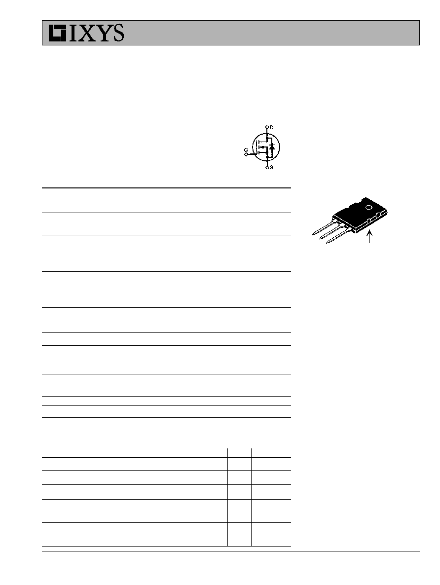
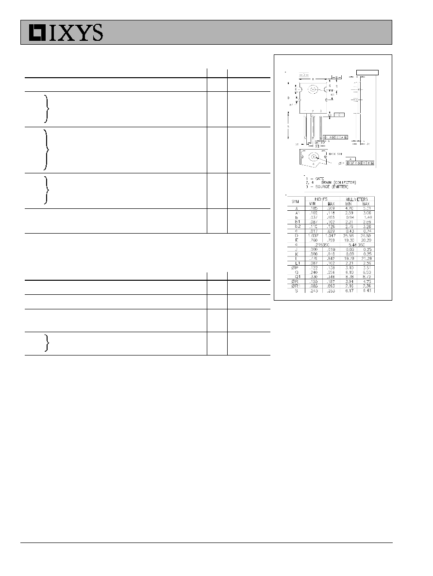
TO-264
10
g
G = Gate
D = Drain
S = Source
TAB = Drain
DS99130E(12/05)
Symbol
Test Conditions
Characteristic Values
(T
J
= 25
° C, unless otherwise specified)
Min. Typ.
Max.
BV
DSS
V
GS
= 0 V, I
D
= 250
µA
300
V
V
GS(th)
V
DS
= V
GS
, I
D
= 500
µA
2.5
5.0
V
I
GSS
V
GS
=
±20 V
DC
, V
DS
= 0
±200
nA
I
DSS
V
DS
= V
DSS
25
µA
V
GS
= 0 V
T
J
= 125
° C
250
µA
R
DS(on)
V
GS
= 10 V, I
D
= 0.5 I
D25
33
m
Pulse test, t
300 µs, duty cycle d 2 %
PolarHT
TM
Power MOSFET
IXTK 102N30P
N-Channel Enhancement Mode
Avalanche Rated
Features
l
International standard package
l
Unclamped Inductive Switching (UIS)
rated
l
Low package inductance
- easy to drive and to protect
Advantages
l
Easy to mount
l
Space savings
l
High power density
V
DSS
= 300 V
I
D25
= 102 A
R
DS(on)
33 m
TO-264 (IXTK)
G
D
S
(TAB)
IXYS reserves the right to change limits, test conditions, and dimensions.
IXTK 102N30P
Symbol
Test Conditions Characteristic Values
(T
J
= 25
° C, unless otherwise specified)
Min.
Typ.
Max.
g
fs
V
DS
= 10 V; I
D
= 0.5 I
D25
, pulse test
45
57
S
C
iss
7500
pF
C
oss
V
GS
= 0 V, V
DS
= 25 V, f = 1 MHz
1150
pF
C
rss
230
pF
t
d(on)
30
ns
t
r
V
GS
= 10 V, V
DS
= 0.5 V
DSS
, I
D
= 60 A
28
ns
t
d(off)
R
G
= 3.3
(External)
130
ns
t
f
30
ns
Q
g(on)
224
nC
Q
gs
V
GS
= 10 V, V
DS
= 0.5 V
DSS
, I
D
= 0.5 I
D25
50
nC
Q
gd
110
nC
R
thJC
0.18
° C/W
R
thCS
0.15
° C/W
Source-Drain Diode Characteristic Values
(T
J
= 25
° C, unless otherwise specified)
Symbol
Test Conditions
Min.
Typ.
Max.
I
S
V
GS
= 0 V
102
A
I
SM
Repetitive
250
A
V
SD
I
F
= I
S
, V
GS
= 0 V,
1.5
V
Pulse test, t
300 µs, duty cycle d 2 %
t
rr
I
F
= 25 A, -di/dt = 100 A/
µs
250
ns
Q
RM
V
R
= 100 V, V
GS
= 0 V
3.3
µC
IXYS MOSFETs and IGBTs are covered by 4,835,592
4,931,844
5,049,961
5,237,481
6,162,665
6,404,065 B1
6,683,344
6,727,585
one or moreof the following U.S. patents:
4,850,072
5,017,508
5,063,307
5,381,025
6,259,123 B1
6,534,343
6,710,405B2
6,759,692
4,881,106
5,034,796
5,187,117
5,486,715
6,306,728 B1
6,583,505
6,710,463
6,771,478 B2
TO-264 (IXTK) Outline
© 2006 IXYS All rights reserved
IXTK 102N30P
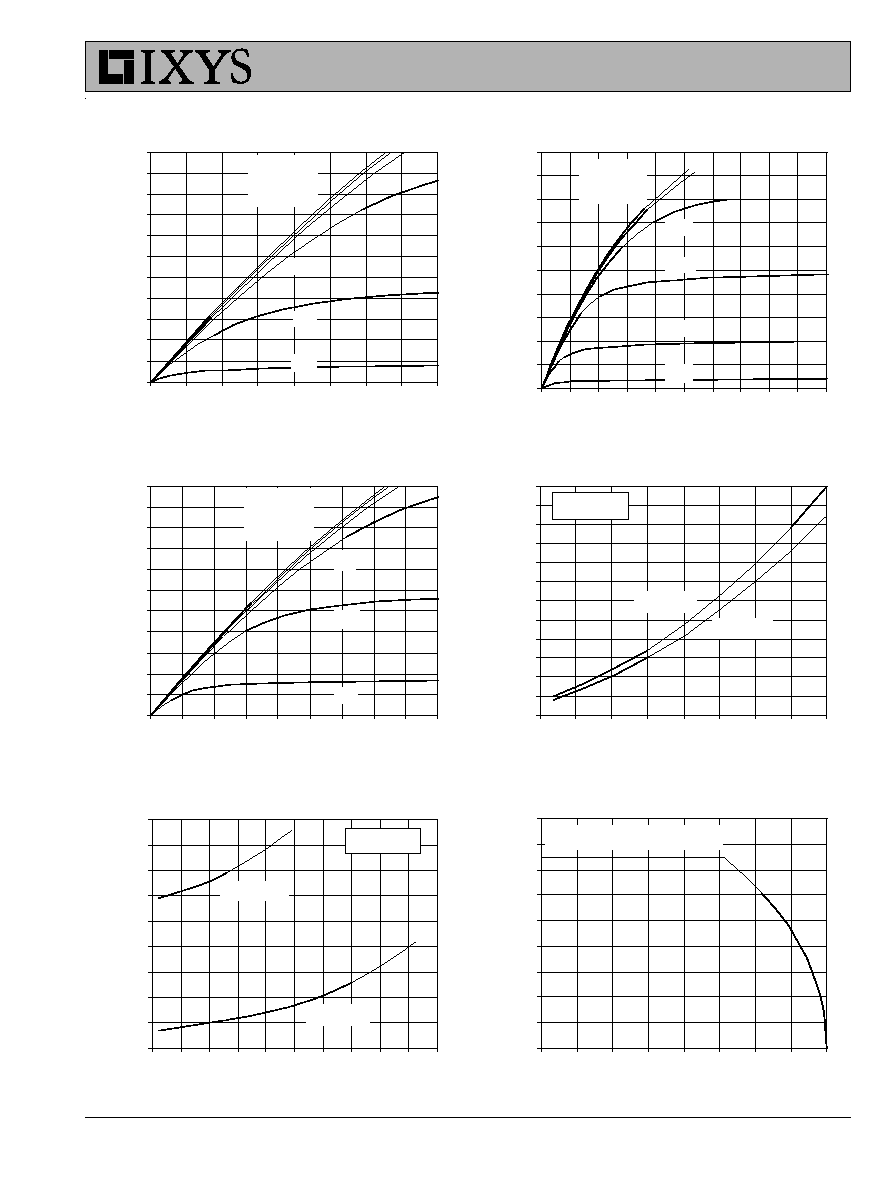
Fig. 2. Exte nde d Output Characte ris tics
@ 25
º
C
0
25
50
75
100
125
150
175
200
225
250
0
2
4
6
8
10
12
14
16
18
20
V
DS
- V olts
I
D
-
A
m
per
es
V
GS
= 10V
9V
7V
6V
8V
5V
Fig. 3. Output Characte ris tics
@ 125
º
C
0
10
20
30
40
50
60
70
80
90
100
110
0
1
2
3
4
5
6
7
8
9
V
DS
- V olts
I
D
-
A
m
per
es
V
GS
= 10V
9V
8V
5V
6V
7V
Fig. 1. Output Characte ris tics
@ 25
º
C
0
10
20
30
40
50
60
70
80
90
100
110
0
0.5
1
1.5
2
2.5
3
3.5
4
V
DS
- V olts
I
D
- A
m
p
e
re
s
V
GS
= 10V
9V
8V
7V
6V
5V
Fig. 4. R
DS(on
)
Norm alize d to 0.5 I
D25
V alue vs . Junction Te m pe rature
0.4
0.6
0.8
1
1.2
1.4
1.6
1.8
2
2.2
2.4
2.6
2.8
-50
-25
0
25
50
75
100
125
150
T
J
- Degrees Centigrade
R
D
S
(
on)
-
N
o
r
m
a
liz
e
d
I
D
= 102A
I
D
= 51A
V
GS
= 10V
Fig. 6. Drain Curre nt vs . Cas e
Te m pe rature
0
10
20
30
40
50
60
70
80
90
-50
-25
0
25
50
75
100
125
150
T
C
- Degrees Centigrade
I
D
- A
m
p
e
re
s
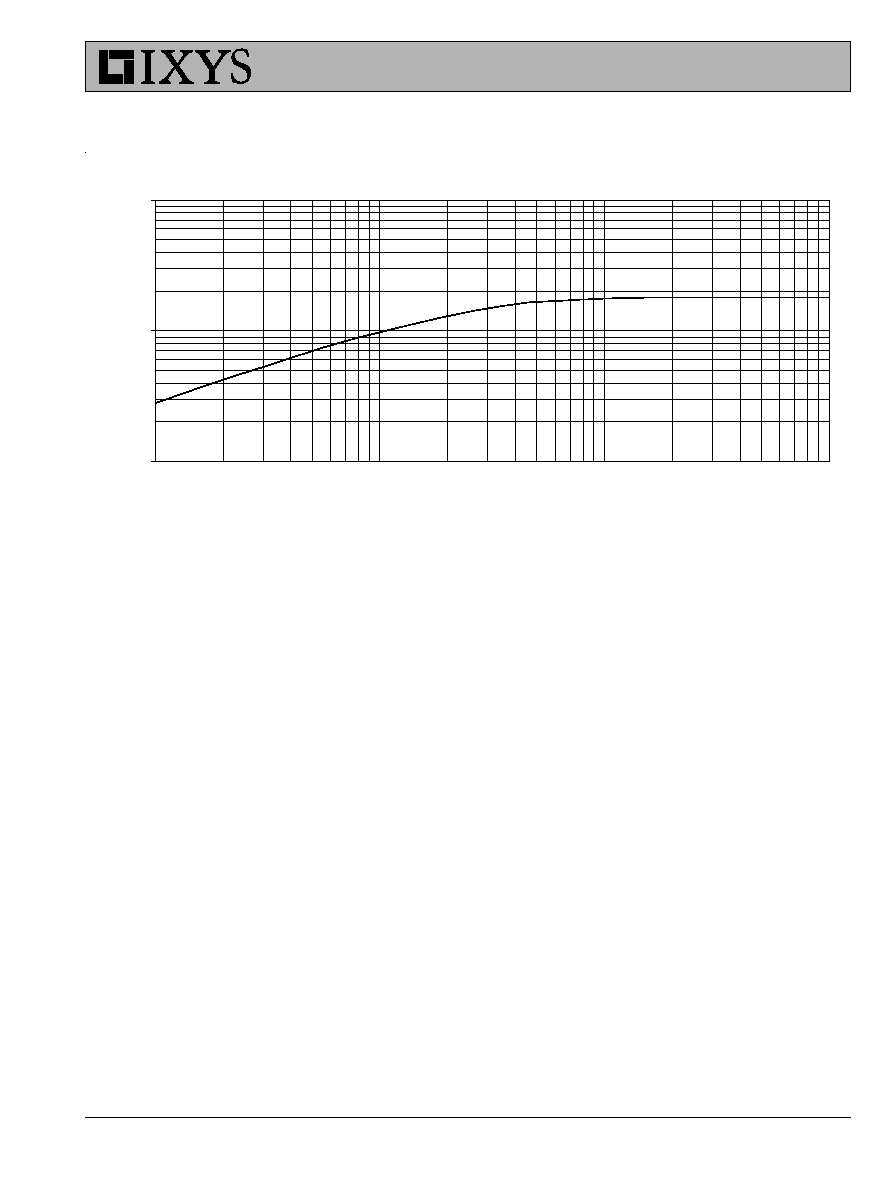
External Lead Current Limit
Fig. 5. R
DS(on)
Norm alize d to
0.5 I
D25
V alue vs . I
D
0.8
1
1.2
1.4
1.6
1.8
2
2.2
2.4
2.6
0
25
50
75
100 125 150 175 200 225 250
I
D
- A mperes
R
DS
(
o
n
)
-
N
o
r
m
a
liz
e
d
T
J
= 125ºC
T
J
= 25ºC
V
GS
= 10V
IXYS reserves the right to change limits, test conditions, and dimensions.
IXTK 102N30P
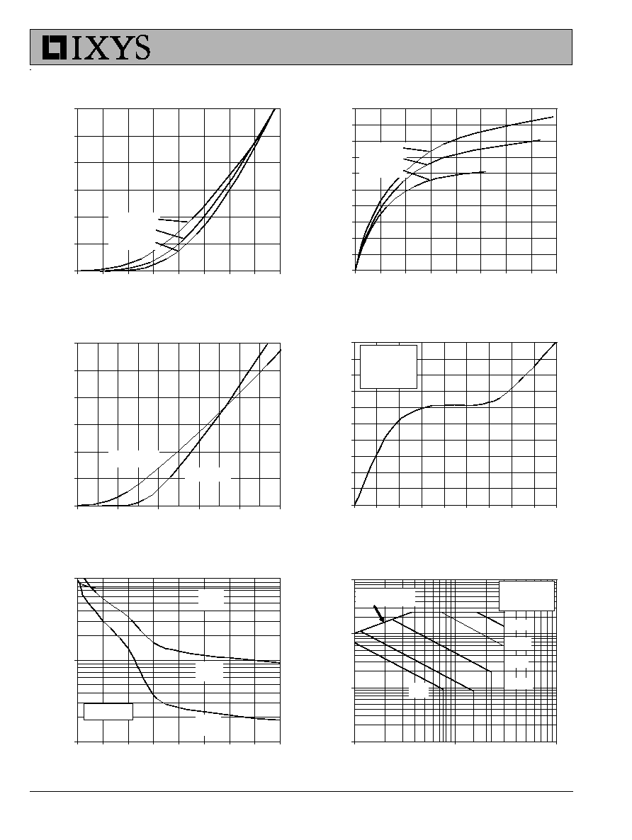
Fig. 11. Capacitance
100
1000
10000
0
5
10
15
20
25
30
35
40
V
DS
- V olts
C
apac
i
t
anc
e -
pi
c
o
F
a
r
ads
C iss
C oss
C rss
f = 1MH z
Fig. 10. Gate Charge
0
1
2
3
4
5
6
7
8
9
10
0
25
50
75
100
125
150
175
200
225
Q
G
- nanoCoulombs
V
G S
- V
o
l
t
s
V
DS
= 150V
I
D
= 51A
I
G
= 10m A
Fig. 7. Input Adm ittance
0
25
50
75
100
125
150
3.5
4
4.5
5
5.5
6
6.5
7
7.5
V
GS
- Volts
I
D
-
A
m
per
es
T
J
= 125ºC
25ºC
-40ºC
Fig. 8. Trans conductance
0
10
20
30
40
50
60
70
80
90
100
0
25
50
75
100
125
150
175
200
I
D
- Amperes
g
fs
-
S
i
em
ens
T
J
= -40ºC
25ºC
125ºC
Fig. 9. Source Curre nt vs .
Source -To-Drain V oltage
0
50
100
150
200
250
300
0.4
0.6
0.8
1
1.2
1.4
V
SD
- V olts
I
S
- A
m
p
e
re
s
T
J
= 125ºC
T
J
= 25ºC
Fig. 12. Forw ard-Bias
Safe Ope rating Are a
1
10
100
1000
10
100
1000
V
DS
- V olts
I
D
-
A
m
per
es
100µs
1m s
D C
T
J
= 150ºC
T
C
= 25ºC
R
DS(on)
Lim it
10m s
25µs
© 2006 IXYS All rights reserved
IXTK 102N30P
Fig. 13. M axim um Trans ie nt The rm al Re s is tance
0.01
0.10
1.00
1
10
100
1000
Pulse Width - milliseconds
R
(t
h
)
J
C
-
ºC/W