© 2002 IXYS All rights reserved
Advance Technical Information
Symbol
Test Conditions
Characteristic Values
(T
J
= 25°C unless otherwise specified)
Min. Typ.
Max.
V
DSS
V
GS
= 0 V, I
D
= 1 mA
250
V
V
GS(th)
V
DS
= V
GS
, I
D
= 250
µ
A
2. 0
4. 0
V
I
GSS
V
GS
= ±20 V DC, V
DS
= 0
±200
nA
I
DSS
V
DS
= V
DSS
T
J
= 25°C
50
µ
A
V
GS
= 0 V
T
J
= 125°C
3
mA
R
DS(on)
V
GS
= 10 V, I
D
= 0.5 I
D25
22 m
Pulse test, t
300 ms, duty cycle d
2%
Features
·
Low R
DS (on)
HDMOS
TM
process
·
Rugged polysilicon gate cell structure
·
International standard package
·
Fast switching times
Applications
·
Motor controls
·
DC choppers
·
Switched-mode power supplies
Advantages
·
Easy to mount with one screw
(isolated mounting screw hole)
·
Space savings
·
High power density
98879A (02/02)
High Current
MegaMOS
TM
FET
N-Channel Enhancement Mode
Symbol
Test conditions
Maximum ratings
V
DSS
T
J
= 25°C to 150°C
250
V
V
DGR
T
J
= 25°C to 150°C; R
GS
= 1.0 M
250
V
V
GS
Continuous
±20
V
V
GSM
Transient
±30
V
I
D25
T
C
= 25
°
C MOSFET chip capability
120
A
I
D(RMS)
External lead current limit
75
A
I
DM
T
C
= 25
°
C, pulse width limited by T
JM
480
A
I
AR
T
C
= 25
°
C
90
A
E
AR
T
C
= 25
°
C
64
mJ
E
AS
T
C
= 25
°
C
3. 0
J
dv/dt
I
S
I
DM
, di/dt
100 A/
µ
s, V
DD
V
DSS
5
V/ns
T
J
150
°
C, R
G
= 2
P
D
T
C
= 25
°
C
560
W
T
J
-55 ... +150
°
C
T
JM
150
°
C
T
stg
-55 ... +150
°
C
T
L
1.6 mm (0.063 in.) from case for 10 s
300
°
C
M
d
Mounting torque
0.7/6
Nm/lb.in.
Weight
TO-264
10
g
TO-264 AA (IXTK)
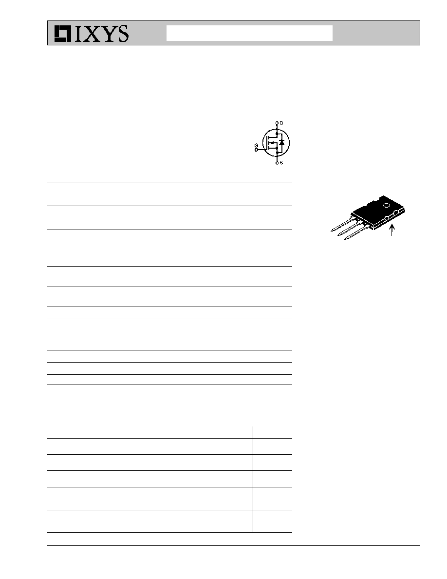
S
G
D
D (TAB)
G = Gate
D
= Drain
S = Source
Tab = Drain
IXTK 120N25
V
DSS
= 250 V
I
D25
= 120 A
R
DS(on)
= 22 m
IXYS reserves the right to change limits, test conditions, and dimensions.
IXYS MOSFETS and IGBTs are covered by one or more of the following U.S. patents:
4,835,592
4,881,106
5,017,508
5,049,961
5,187,117
5,486,715
6,306,728B1
4,850,072
4,931,844
5,034,796
5,063,307
5,237,481
5,381,025
Symbol
Test Conditions
Characteristic values
(T
J
= 25°C unless otherwise specified)
Min.
Typ. Max.
g
fs
V
DS
= 10 V; I
D
= 0.5 I
D25
, pulse test
65
85
S
C
iss
9400
pF
C
oss
V
GS
= 0 V, V
DS
= 25 V, f = 1 MHz
1730
pF
C
rss
550
pF
t
d(on)
35
ns
t
r
V
GS
= 10 V, V
DS
= 0.5 V
DSS
, I
D
= 0.5 I
D25
38
ns
t
d(off)
R
G
= 1.5
(External)
175
ns
t
f
35
ns
Q
g(on)
400
nC
Q
gs
V
GS
= 10 V, V
DS
= 0.5 V
DSS
, I
D
= 0.5 I
D25
70
nC
Q
gd
155
nC
R
thJC
0.22 K/W
R
thCK
0.15
K/W
Source-Drain Diode
Ratings and Characteristics
(T
J
= 25°C unless otherwise specified)
Symbol
Test Conditions
Min.
Typ. Max.
I
S
V
GS
= 0V
120
A
I
SM
Repetitive; pulse width limited by T
JM
480
A
V
SD
I
F
= I
S
, V
GS
= 0 V,
1.5
V
Pulse test, t
300 µs, duty cycle d
2 %
t
rr
I
F
= 30A, -di/dt = 100 A/µs, V
R
= 100V
350
ns
Q
rr
6
µ
C
IXTK 120N25
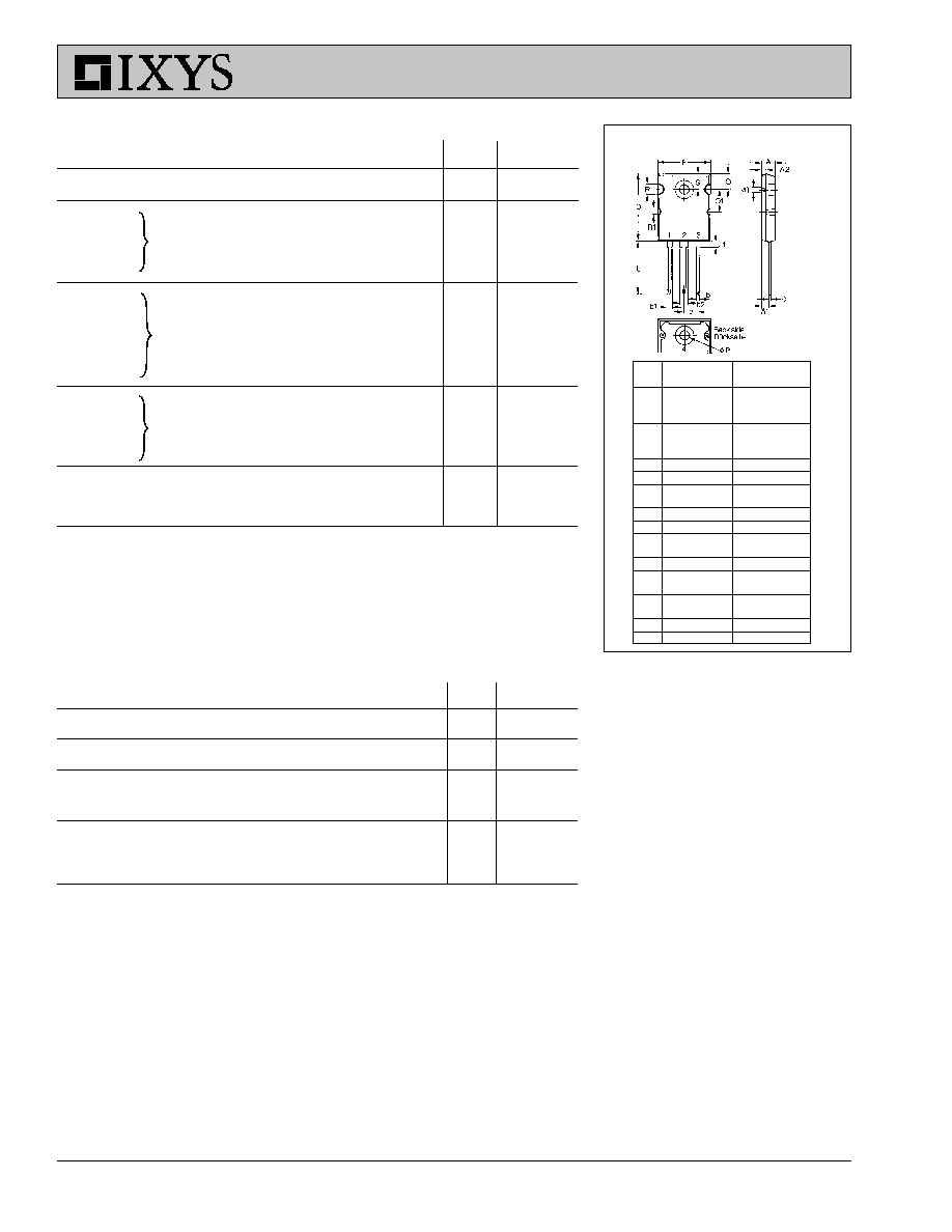
TO-264 AA Outline
Millimeter
Inches
Min.
Max.
Min.
Max.
A
4.82
5.13
.190
.202
A1
2.54
2.89
.100
.114
A2
2.00
2.10
.079
.083
b
1.12
1.42
.044
.056
b1
2.39
2.69
.094
.106
b2
2.90
3.09
.114
.122
c
0.53
0.83
.021
.033
D
25.91
26.16
1.020
1.030
E
19.81
19.96
.780
.786
e
5.46 BSC
.215 BSC
J
0.00
0.25
.000
.010
K
0.00
0.25
.000
.010
L
20.32
20.83
.800
.820
L1
2.29
2.59
.090
.102
P
3.17
3.66
.125
.144
Q
6.07
6.27
.239
.247
Q1
8.38
8.69
.330
.342
R
3.81
4.32
.150
.170
R1
1.78
2.29
.070
.090
S
6.04
6.30
.238
.248
T
1.57
1.83
.062
.072
Dim.