1 - 4
© 2000 IXYS All rights reserved
Symbol
Test Conditions
Maximum Ratings
IXTK
IXTN
V
DSS
T
J
= 25
°
C to 150
°
C
1000
1000
V
V
DGR
T
J
= 25
°
C to 150
°
C; R
GS
= 1 M
1000
1000
V
V
GS
Continuous
±
20
±
20
V
V
GSM
Transient
±
30
±
30
V
I
D25
T
C
= 25
°
C, Chip capability
21
21
A
I
DM
T
C
= 25
°
C, pulse width limited by T
JM
84
84
A
P
D
T
C
= 25
°
C
500
520
W
T
J
-55 ... +150
°
C
T
JM
150
°
C
T
stg
-55 ... +150
°
C
T
L
1.6 mm (0.063 in) from case for 10 s
300
-
°
C
V
ISOL
50/60 Hz, RMS
t = 1 min
-
2500
V~
I
ISOL
1 mA
t = 1 s
-
3000
V~
M
d
Mounting torque
0.9/6
1.5/13
Nm/lb.in.
Terminal connection torque
-
1.5/13
Nm/lb.in.
Weight
10
30
g
IXTK 21N100
V
DSS
= 1000 V
IXTN 21N100
I
D25
= 21 A
R
DS(on)
= 0.55
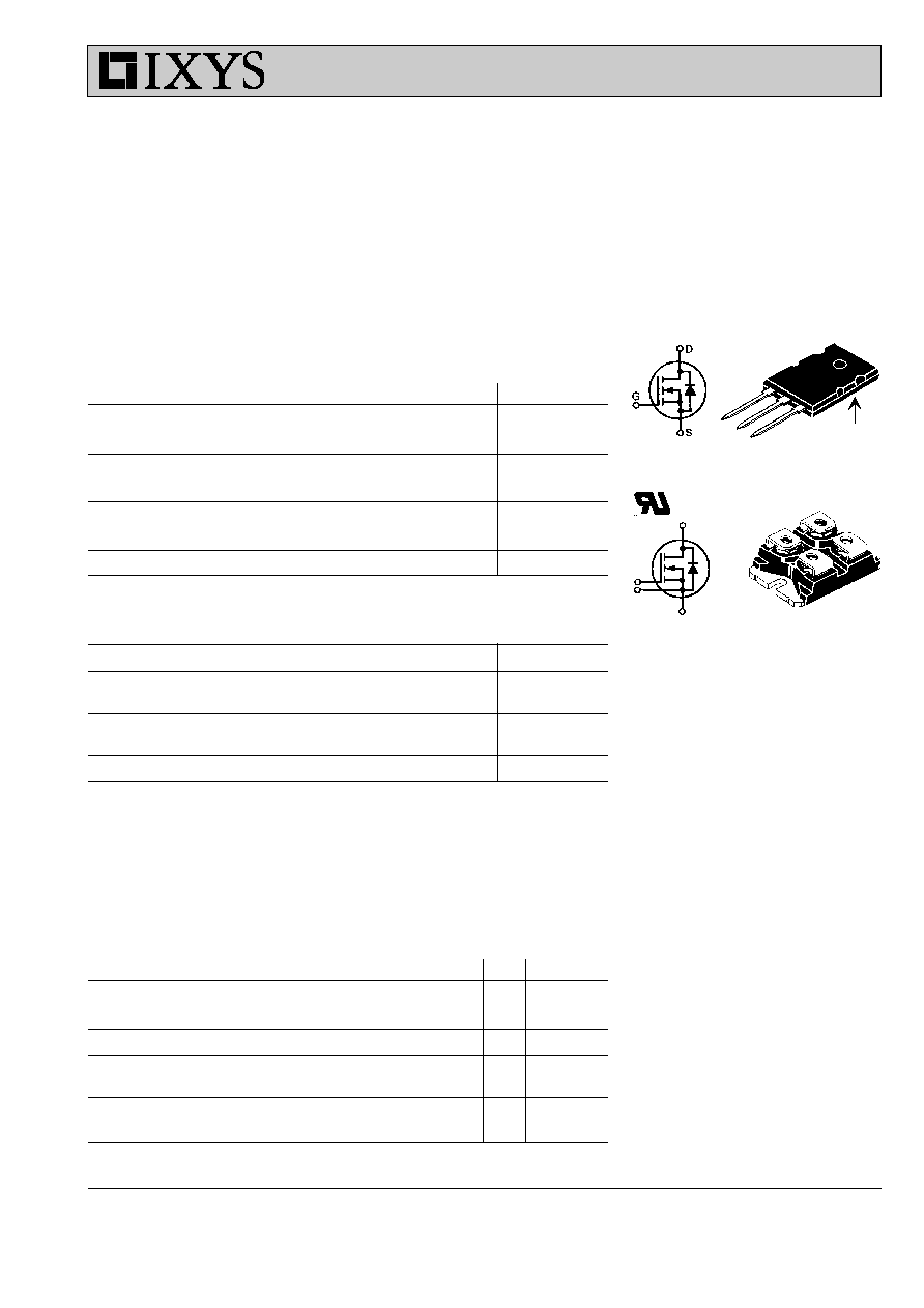
TO-264 AA (IXTK)
S
G
D
D
S
G
S
G = Gate
D = Drain
S = Source
TAB = Drain
Either Source terminal at miniBLOC can be used
as Main or Kelvin Source
S
G
S
D
N-Channel, Enhancement Mode
Symbol
Test Conditions
Characteristic Values
(T
J
= 25
°
C, unless otherwise specified)
min.
typ.
max.
V
DSS
V
GS
= 0 V, I
D
= 6 mA
1000
V
V
GH(th)
V
DS
= V
GS
, I
D
= 500
µ
A
2
4.5
V
I
GSS
V
GS
=
±
20 V
DC
, V
DS
= 0
±
200
nA
I
DSS
V
DS
= 0.8 · V
DSS
T
J
= 25
°
C
500
µ
A
V
GS
= 0 V
T
J
= 125
°
C
2
mA
R
DS(on)
V
GS
= 10 V, I
D
= 0.5 · I
D25
0.55
Pulse test, t
300
µ
s, duty cycle d
2 %
92808I(5/97)
Features
l
International standard packages
l
JEDEC
TO-264,
epoxy
meet
UL
94
V-0
flammability classification
l
miniBLOC,
(ISOTOP-compatible) with
Aluminium nitride isolation
l
Low R
DS (on)
HDMOS
TM
process
l
Rugged polysilicon gate cell structure
l
Low package inductance
Applications
l
DC-DC converters
l
Synchronous rectification
l
Battery chargers
l
Switched-mode and resonant-mode
power supplies
l
DC choppers
l
Temperature and lighting controls
Advantages
l
Easy to mount
l
Space savings
l
High power density
D (TAB)
miniBLOC, SOT-227 B
E153432
High Voltage
MegaMOS
TM
FETs
IXYS reserves the right to change limits, test conditions, and dimensions.
2 - 4
© 2000 IXYS All rights reserved
Symbol
Test Conditions
Characteristic Values
(T
J
= 25
°
C, unless otherwise specified)
min.
typ.
max.
g
fs
V
DS
= 10 V; I
D
= 0.5 · I
D25
, pulse test
24
S
C
iss
8400
pF
C
oss
V
GS
= 0 V, V
DS
= 25 V, f = 1 MHz
630
pF
C
rss
110
pF
t
d(on)
30
ns
t
r
V
GS
= 10 V, V
DS
= 0.5 · V
DSS
, I
D
= 0.5 · I
D25
50
ns
t
d(off)
R
G
= 1
(External),
100
ns
t
f
40
ns
Q
g(on)
250
nC
Q
gs
V
GS
= 10 V, V
DS
= 0.5 · V
DSS
, I
D
= 0.5 · I
D25
60
nC
Q
g d
100
nC
R
thJC
TO-264 AA
0.25
K/W
R
thCK
TO-264 AA
0.15
K/W
R
thJC
miniBLOC, SOT-227 B
0.24
K/W
R
thCK
miniBLOC, SOT-227 B
0.05
K/W
Source-Drain Diode
Characteristic Values
(T
J
= 25
°
C, unless otherwise specified)
Symbol
Test Conditions
min.
typ.
max.
I
S
V
GS
= 0 V
21
A
I
SM
Repetitive; pulse width limited by T
JM
84
A
V
SD
I
F
= I
S
, V
GS
= 0 V,
1.5
V
Pulse test, t
300
µ
s, duty cycle d
2 %
t
rr
1000
ns
I
RM
20
A
I
F
= I
S
, -di/dt = 100 A/
µ
s, V
R
= 100 V
IXTK 21N100
IXTN 21N100
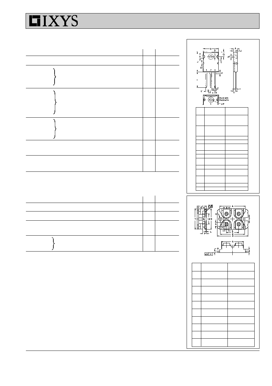
TO-264 AA Outline
Millimeter
Inches
Min.
Max.
Min.
Max.
A
4.82
5.13
.190
.202
A1
2.54
2.89
.100
.114
A2
2.00
2.10
.079
.083
b
1.12
1.42
.044
.056
b1
2.39
2.69
.094
.106
b2
2.90
3.09
.114
.122
c
0.53
0.83
.021
.033
D
25.91
26.16
1.020
1.030
E
19.81
19.96
.780
.786
e
5.46 BSC
.215 BSC
J
0.00
0.25
.000
.010
K
0.00
0.25
.000
.010
L
20.32
20.83
.800
.820
L1
2.29
2.59
.090
.102
P
3.17
3.66
.125
.144
Q
6.07
6.27
.239
.247
Q1
8.38
8.69
.330
.342
R
3.81
4.32
.150
.170
R1
1.78
2.29
.070
.090
S
6.04
6.30
.238
.248
T
1.57
1.83
.062
.072
Dim.
miniBLOC, SOT-227 B
M4 screws (4x) supplied
Dim.
Millimeter
Inches
Min.
Max.
Min.
Max.
A
31.50
31.88
1.240
1.255
B
7.80
8.20
0.307
0.323
C
4.09
4.29
0.161
0.169
D
4.09
4.29
0.161
0.169
E
4.09
4.29
0.161
0.169
F
14.91
15.11
0.587
0.595
G
30.12
30.30
1.186
1.193
H
38.00
38.23
1.496
1.505
J
11.68
12.22
0.460
0.481
K
8.92
9.60
0.351
0.378
L
0.76
0.84
0.030
0.033
M
12.60
12.85
0.496
0.506
N
25.15
25.42
0.990
1.001
O
1.98
2.13
0.078
0.084
P
4.95
5.97
0.195
0.235
Q
26.54
26.90
1.045
1.059
R
3.94
4.42
0.155
0.174
S
4.72
4.85
0.186
0.191
T
24.59
25.07
0.968
0.987
U
-0.05
0.1
-0.002
0.004
IXYS MOSFETS and IGBTs are covered by one or more of the following U.S. patents:
4,835,592
4,881,106
5,017,508
5,049,961
5,187,117
5,486,715
4,850,072
4,931,844
5,034,796
5,063,307
5,237,481
5,381,025
3 - 4
© 2000 IXYS All rights reserved
IXTK 21N100
IXTN 21N100
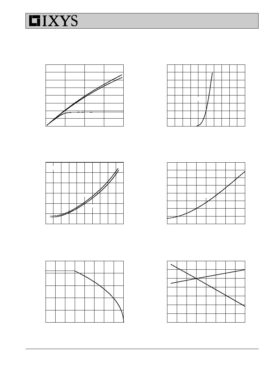
Fig. 1 Output Characteristics
Fig. 2 Input Admittance
Fig. 3 R
DS(on)
vs. Drain Current
Fig. 4 Temperature Dependence
of Drain to Source Resistance
Fig. 5 Drain Current vs.
Fig. 6 Temperature Dependence of
Case Temperature
Breakdown and Threshold Voltage
T
J
- Degrees C
-50
-25
0
25
50
75
100 125 150
BV/
V
G(
t
h
)
- No
rm
a
liz
e
d
0.5
0.6
0.7
0.8
0.9
1.0
1.1
1.2
V
GS(th)
T
C
- Degrees C
-50
-25
0
25
50
75
100 125 150
I
D
-
Am
per
es
0
5
10
15
20
25
T
J
- Degrees C
-50
-25
0
25
50
75
100 125 150
R
DS
(on)
- No
rm
a
liz
e
d
0.50
0.75
1.00
1.25
1.50
1.75
2.00
2.25
2.50
I
D
- Amperes
0
5
10
15 20 25 30
35 40 45 50
R
DS
(on)
- No
rm
a
liz
e
d
0.9
1.0
1.1
1.2
1.3
1.4
1.5
V
GS
- Volts
0
1
2
3
4
5
6
7
8
9
10
I
D
-
Am
per
es
0
5
10
15
20
25
30
35
40
V
DS
- Volts
0
5
10
15
20
I
D
-
Am
per
es
0
5
10
15
20
25
30
35
40
6V
BV
DSS
I
D
= 12A
T
J
= 25°C
V
GS
= 15V
V
GS
= 10V
5V
V
GS
= 10V
T
J
= 25°C
T
J
= 25°C
4 - 4
© 2000 IXYS All rights reserved
IXTK 21N100
IXTN 21N100
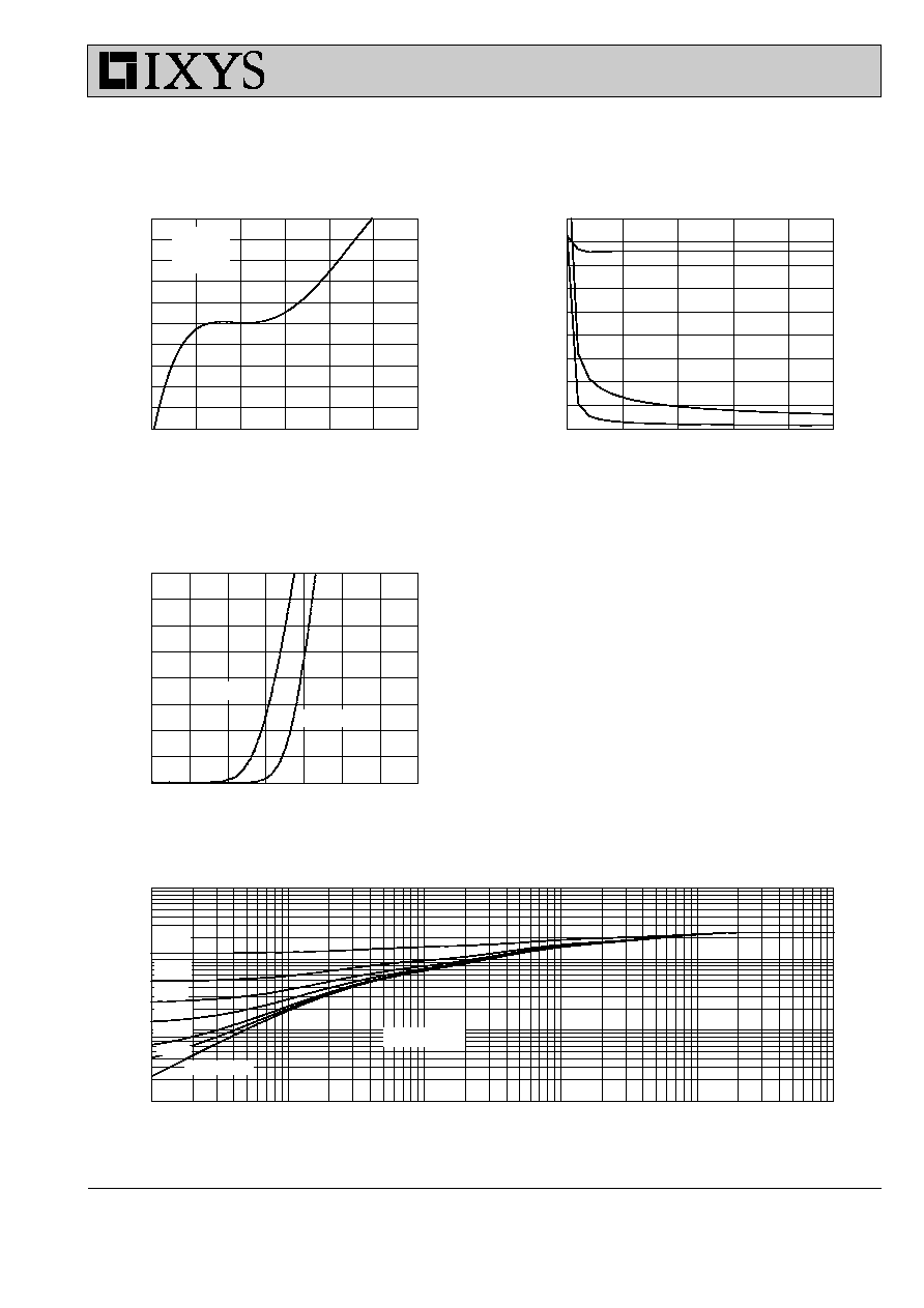
Fig.7 Gate Charge Characteristic Curve
Fig.8 Capacitance Curves
Fig.10 Transient Thermal Impedance
Fig.9 Source Current vs. Source
to Drain Voltage
Pulse Width - Seconds
0.0001
0.001
0.01
0.1
1
10
R(t
h
)
JC
-
K
/
W
0.001
0.01
0.1
1
V
SD
- Volts
0.0
0.2
0.4
0.6
0.8
1.0
1.2
1.4
I
D
-
Am
per
es
0
5
10
15
20
25
30
35
40
V
DS
- Volts
0
5
10
15
20
C
apaci
t
ance -
pF
0
1000
2000
3000
4000
5000
6000
7000
8000
9000
C
rss
C
oss
Gate Charge - nCoulombs
0
50
100
150
200
250
300
V
GS
- V
o
l
t
s
0
1
2
3
4
5
6
7
8
9
10
V
DS
= 500V
I
D
= 12A
I
G
= 10mA
C
iss
f = 1 MHz
V
DS
= 25V
T
J
= 125°C
T
J
= 25°C
Single pulse
D = Duty Cycle
D=0.1
D=0.05
D=0.02
D=0.01
D=0.2
D=0.5