 | –≠–ª–µ–∫—Ç—Ä–æ–Ω–Ω—ã–π –∫–æ–º–ø–æ–Ω–µ–Ω—Ç: IXTP3N110 | –°–∫–∞—á–∞—Ç—å:  PDF PDF  ZIP ZIP |
© 2001 IXYS All rights reserved
N-Channel Enhancement Mode
Avalanche Rated, High dv/dt
Features
l
International standard packages
l
Low R
DS (on)
l
Rated for unclamped Inductive load
Switching (UIS)
l
Molding epoxies meet UL
94
V-0
flammability classification
Advantages
l
Easy to mount
l
Space savings
l
High power density
High Voltage
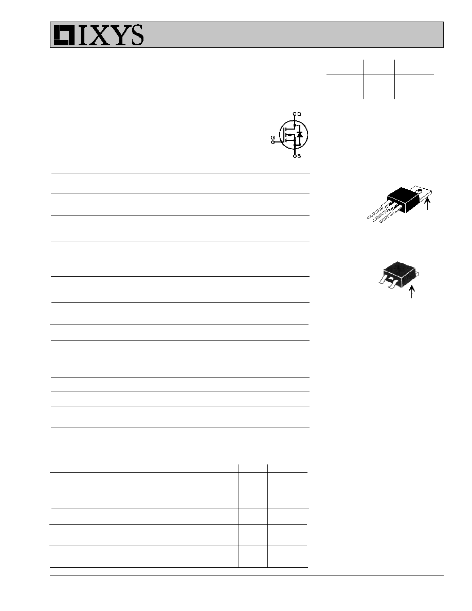
Power MOSFETs
G
S
TO-263 (IXTA)
G D
S
TO-220 (IXTP)
G = Gate
D = Drain
S = Source
TAB = Drain
IXTA/IXTP 3N120
IXTA/IXTP 3N110
D (TAB)
D (TAB)
V
DSS
I
D25
R
DS(on)
1200 V 3 A
4.5
1100 V 3 A
4.0
Symbol
Test Conditions
Maximum Ratings
V
DSS
T
J
= 25
∞
C to 150
∞
C
3N120
1200
V
3N110
1100
V
V
DGR
T
J
= 25
∞
C to 150
∞
C; R
GS
= 1 M
3N120
1200
V
3N110
1100
V
V
GS
Continuous
±
20
V
V
GSM
Transient
±
30
V
I
D25
T
C
= 25
∞
C
3
A
I
DM
T
C
= 25
∞
C, pulse width limited by T
JM
12
A
I
AR
T
C
= 25
∞
C
3
A
E
AR
T
C
= 25
∞
C
20
mJ
E
AS
700
mJ
dv/dt
I
S
I
DM
, di/dt
100 A/
µ
s, V
DD
V
DSS
,
5
V/ns
T
J
150
∞
C, R
G
= 2
P
D
T
C
= 25
∞
C
150
W
T
J
-55 to +150
∞
C
T
JM
150
∞
C
T
stg
-55 to +150
∞
C
T
L
1.6 mm (0.063 in) from case for 10 s 300
∞
C
M
d
Mounting torque (TO-220)
1.13/10 Nm/lb.in.
Weight
TO-220 4
g
TO-263 2
g
Symbol
Test Conditions
Characteristic Values
(T
J
= 25
∞
C, unless otherwise specified)
min.
typ.
max.
V
DSS
V
GS
= 0 V, I
D
= 1 mA
3N120
1200
V
3N110
1100
V
V
GS(th)
V
DS
= V
GS
, I
D
= 250
µ
A
2.5
4.5
V
I
GSS
V
GS
=
±
20 V
DC
, V
DS
= 0
±
100
nA
I
DSS
V
DS
= 0.8 V
DSS
T
J
= 25
∞
C
25
µ
A
V
GS
= 0 V
T
J
= 125
∞
C
1
mA
R
DS(on)
V
GS
= 10 V, I
D
= 0.5 I
D25
3N120
4.5
Note 1
3N110
4.0
Preliminary Data Sheet
98844A (11/01)
IXYS MOSFETS and IGBTs are covered by one or more of the following U.S. patents:
4,835,592
4,881,106
5,017,508
5,049,961
5,187,117
5,486,715
4,850,072
4,931,844
5,034,796
5,063,307
5,237,481
5,381,025
IXYS reserves the right to change limits, test conditions, and dimensions.
IXTA/IXTP 3N120
IXTA/IXTP 3N110
Symbol
Test Conditions
Characteristic Values
(T
J
= 25
∞
C, unless otherwise specified)
min.
typ.
max.
g
fs
V
DS
= 10 V; I
D
= 0.5 ∑ I
D25
, Note 1
1.5
2.2
S
C
iss
1050 1300
pF
C
oss
V
GS
= 0 V, V
DS
= 25 V, f = 1 MHz
100 125
pF
C
rss
25
50
pF
t
d(on)
17
ns
t
r
V
GS
= 10 V, V
DS
= 0.5 ∑ V
DSS
, I
D
= 0.5 ∑ I
D25
15
ns
t
d(off)
R
G
= 4.7
(External),
32
ns
t
f
18
ns
Q
g(on)
39
nC
Q
gs
V
GS
= 10 V, V
DS
= 0.5 ∑ V
DSS
, I
D
= 0.5 ∑ I
D25
9
nC
Q
gd
22
nC
R
thJC
0.8
K/W
R
thCK
(TO-220)
0.25
K/W
Source-Drain Diode
Characteristic Values
(T
J
= 25
∞
C, unless otherwise specified)
Symbol
Test Conditions
min.
typ.
max.
I
S
V
GS
= 0 V
3
A
I
SM
Repetitive; pulse width limited by T
JM
12
A
V
SD
I
F
= I
S
, V
GS
= 0 V, Note 1
1.5
V
t
rr
I
F
= I
S
, -di/dt = 100 A/
µ
s, V
R
= 100 V
700
ns
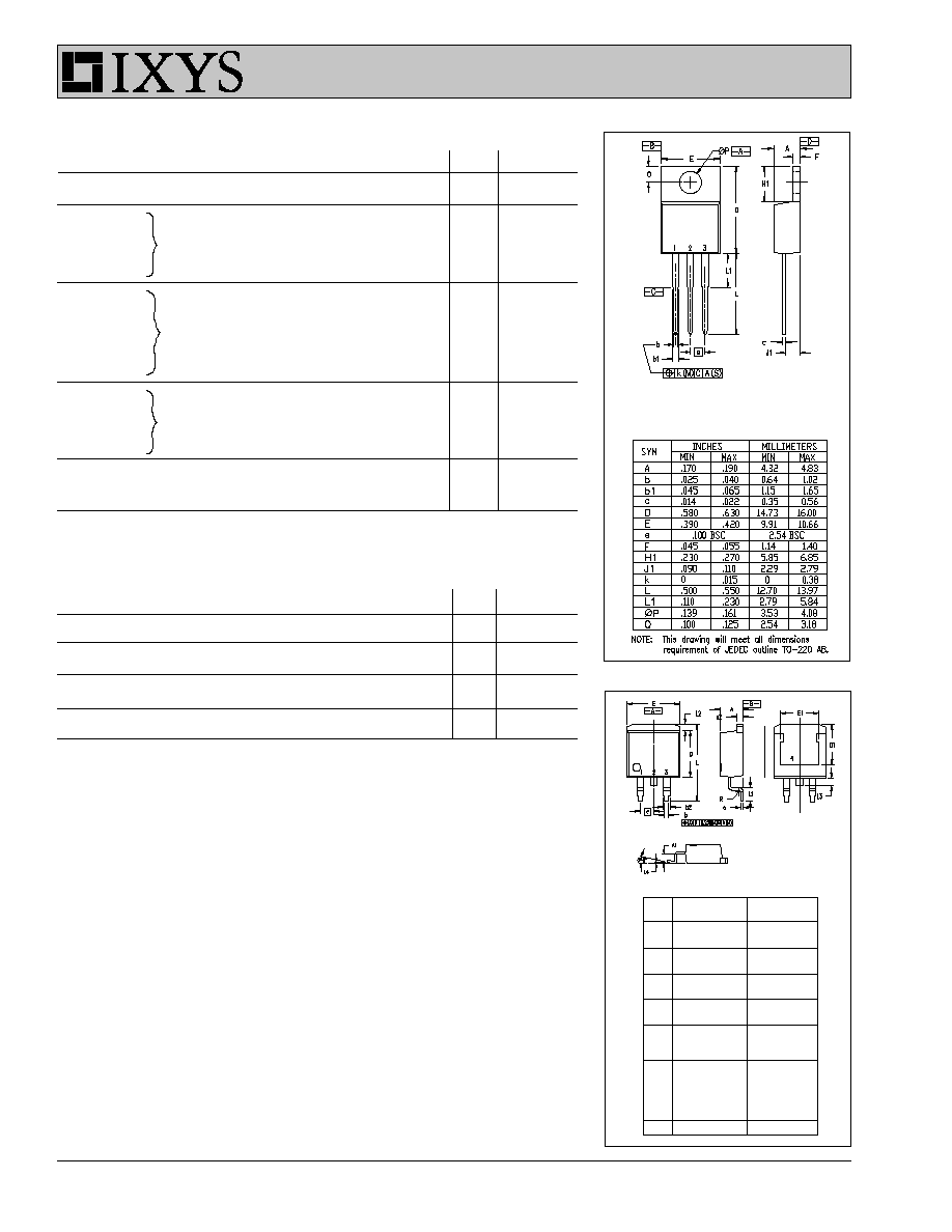
TO-263 (IXTA) Outline
1. Gate
2. Drain
3. Source
4. Drain
Bottom Side
Dim.
Millimeter
Inches
Min.
Max.
Min.
Max.
A
4.06
4.83
.160
.190
A1
2.03
2.79.080
.110
b
0.51
0.99
.020
.039
b2
1.14
1.40
.045
.055
c
0.46
0.74
.018
.029
c2
1.14
1.40
.045
.055
D
8.64
9.65
.340
.380
D1
7.11
8.13
.280
.320
E
9.65
10.29
.380
.405
E1
6.86
8.13
.270
.320
e
2.54
BSC
.100
BSC
L
14.61
15.88
.575
.625
L1
2.292.79
.09
0
.110
L2
1.02
1.40
.040
.055
L3
1.27
1.78
.050
.070
L4
0
0.38
0
.015
R
0.46
0.74
.018
.029
Pins: 1 - Gate
2 - Drain
3 - Source
4 - Drain
Bottom Side
TO-220 (IXTP) Outline
Notes: 1. Pulse test, t
300
µ
s, duty cycle d
2 %
© 2001 IXYS All rights reserved
V
GS
- Volts
3.5
4.0
4.5
5.0
5.5
6.0
I
D
-
A
m
p
e
r
e
s
0.0
0.5
1.0
1.5
2.0
2.5
3.0
T
C
- Degrees C
-50 -25
0
25
50
75
100 125 150
I
D
-
A
m
p
e
r
e
s
0.0
0.5
1.0
1.5
2.0
2.5
3.0
3.5
4.0
T
J
- Degrees C
25
50
75
100
125
150
R
DS(O
N)
- Nor
m
al
iz
ed
1.0
1.3
1.6
1.9
2.2
2.5
2.8
I
D
=1.5A
I
D
- Amperes
0
1
2
3
4
5
R
DS(ON
)
-
Nor
m
al
iz
e
d
0.75
1.00
1.25
1.50
1.75
2.00
2.25
2.50
V
DS
- Volts
0
3
6
9
12 15 18 21 24 27 30
I
D
-
A
m
p
e
r
e
s
0.0
0.5
1.0
1.5
2.0
2.5
3.0
3.5
4.0
V
DS
- Volts
0
2
4
6
8
10 12 14 16 18 20
I
D
- A
m
per
e
s
0
1
2
3
4
5
V
GS
= 10V
T
J
= 125
O
C
T
J
= 25
O
C
4V
4V
5V
T
J
= 25
o
C
I
D
= 3A
T
J
= 125
o
C
V
GS
= 9V
8V
7V
6V
T
J
= 125
O
C
5V
V
GS
= 9V
8V
7V
6V
T
J
= 25
O
C
V
GS
= 10V
IXT_3N110
IXT_3N120
IXTA/IXTP 3N120
IXTA/IXTP 3N110
Fig.1 Output Characteristics @ T
j
= 25∞C
Fig. 2 Output Characteristics @ T
j
= 125∞C
Fig. 3 R
DS(on)
vs. Drain Current
Fig. 4 Temperature Dependence of Drain
to Source Resistance
Fig. 5 Drain Current vs. Case Temperature
Fig. 6 Drain Current vs Gate Source Voltage
IXYS MOSFETS and IGBTs are covered by one or more of the following U.S. patents:
4,835,592
4,881,106
5,017,508
5,049,961
5,187,117
5,486,715
4,850,072
4,931,844
5,034,796
5,063,307
5,237,481
5,381,025
IXYS reserves the right to change limits, test conditions, and dimensions.
IXTA/IXTP 3N120
IXTA/IXTP 3N110
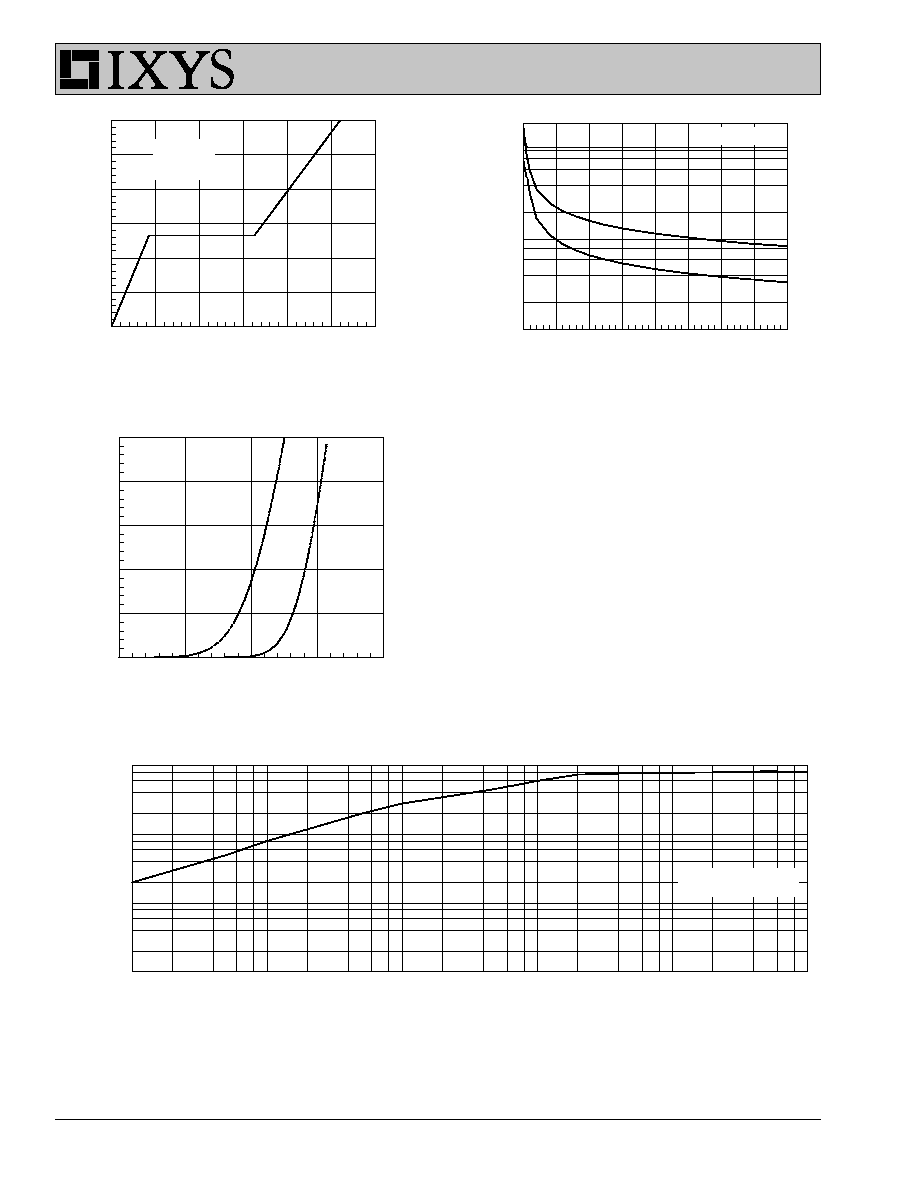
V
SD
- Volts
0.2
0.4
0.6
0.8
1.0
I
D
-
A
m
pe
r
e
s
0
1
2
3
4
5
Pulse Width - Seconds
10
-4
10
-3
10
-2
10
-1
10
0
10
1
R(
th
)
JC
- K/W
0.00
0.01
0.10
1.00
V
DS
- Volts
0
5
10
15
20
25
30
35
40
C
a
pac
i
tance -
pF
10
100
1000
Gate Charge - nC
0
10
20
30
40
50
60
V
GS
- Volts
0
2
4
6
8
10
12
Crss
Coss
Ciss
V
DS
= 600V
I
D
= 1.5A
f = 1MHz
T
J
= 125
O
C
T
J
= 25
O
C
V
GS
= 0V
Single Pulse
Fig. 7 Gate Charge Characteristic Curve
Fig. 8 Capacitance Curves
Fig. 9 Drain Current vs Drain to Source Voltage
Fig.10 Transient Thermal Impedance