
© 2002 IXYS All rights reserved
1 - 2
I
RMS
= 175 A
V
RRM
= 800-1600 V
V
RSM
V
RRM
Type
V
DSM
V
DRM
V
V
800
800
MMO 175-08io7
MLO 175-08io7
1200
1200
MMO 175-12io7
MLO 175-12io7
1600
1600
MMO 175-16io7
MLO 175-16io7
Features
∑ Thyristor controller for AC (circuit
W1C acc. to IEC) for mains frequency
∑ Isolation voltage 3000 V~
∑ Planar glass passivated chips
∑ Low forward voltage drop
∑ Lead suitable for PC board solering
Applications
∑ Switching and control of single and
three phase AC circuits
∑ Light and temperature control
∑ Softstart AC motor controller
∑ Solid state switches
Advantages
∑ Easy to mount with two screws
∑ Space and weight savings
∑ Improved temperature and power
cycling
∑ High power density
∑ Small and light weight
MMO 175
MLO
175
Symbol
Conditions
Maximum Ratings
I
RMS
T
C
= 85įC, 50 - 400 Hz, (per single controller)
175
A
I
TRMS
125
A
I
TAVM
T
C
= 85įC; 180į sine
80
A
I
TSM
T
VJ
= 45įC
t = 10 ms (50 Hz), sine
1500
A
V
R
= 0
t = 8.3 ms (60 Hz), sine
1600
A
T
VJ
= 125įC
t = 10 ms (50 Hz), sine
1350
A
V
R
= 0
t = 8.3 ms (60 Hz), sine
1450
A
I
2
t
T
VJ
= 45įC
t = 10 ms (50 Hz), sine
11200
A
2
s
V
R
= 0
t = 8.3 ms (60 Hz), sine
10750
A
2
s
T
VJ
= 125įC
t = 10 ms (50 Hz), sine
9100
A
2
s
V
R
= 0
t = 8.3 ms (60 Hz), sine
8830
A
2
s
(di/dt)
cr
T
VJ
= 125įC
repetitive, I
T
= 80 A
150
A/Ķs
f = 50 Hz, t
P
= 200 Ķs
V
D
=
2
/
3
V
DRM
I
G
= 0.45 A
non repetitive, I
T
= I
TAVM
500
A/Ķs
di
G
/dt = 0.45 A/Ķs
(dv/dt)
cr
T
VJ
= 125įC; V
DR
=
2
/
3
V
DRM
1000
V/Ķs
R
GK
=
; method 1 (linear voltage rise)
P
GM
T
VJ
= 125įC
t
p
= 30 Ķs
10
W
I
T
= I
TAVM
t
p
= 300 Ķs
5
W
P
GAVM
0.5
W
V
RGM
10
V
T
VJ
-40...+150
įC
T
VJM
150
įC
T
stg
-40...+125
įC
V
ISOL
50/60 Hz, RMS
t = 1 min
2500
V~
I
ISOL
1 mA
t = 1 s
3000
V~
M
d
Mounting torque (M4)
1.5...2.0/14...18 Nm/lb.in.
Weight
typ.
18
g
Data according to IEC 60747 and to a single thyristor/diode unless otherwise stated.
AC Controller Modules
Preliminary Data
241
I / H
G / F
G / F
I / H
A
N
MMO
(W1C)
MLO
(W1H)
A
© 2002 IXYS All rights reserved
2 - 2
Symbol
Conditions
Characteristic Values
I
D
, I
R
T
VJ
= 125įC; V
R
= V
RRM
; V
D
= V
DRM
5
mA
V
T
I
T
= 200 A; T
VJ
= 25įC
1.57
V
V
T0
For power-loss calculations only
0.85
V
r
T
3.7
m
V
GT
V
D
= 6 V
T
VJ
= 25įC
1.5
V
T
VJ
= -40įC
1.6
V
I
GT
V
D
= 6 V
T
VJ
= 25įC
100
mA
T
VJ
= -40įC
200
mA
V
GD
T
VJ
= 125įC; V
D
=
2
/
3
V
DRM
0.2
V
I
GD
10
mA
I
L
T
VJ
= 25įC; t
P
= 10 Ķs
450
mA
I
G
= 0.45 A; di
G
/dt = 0.45 A/Ķs
I
H
T
VJ
= 25įC; V
D
= 6 V; R
GK
=
200
mA
t
gd
T
VJ
= 25įC; V
D
= Ĺ V
DRM
2
Ķs
I
G
= 0.45 A; di
G
/dt = 0.45 A/Ķs
R
thJC
per thyristor; DC
0.5
K/W
per module
0.25
K/W
R
thCH
per thyristor; sine 180į el
typ.
0.12
K/W
per module
typ.
0.06
K/W
d
S
Creeping distance on surface
11.2
mm
d
A
Creepage distance in air
17.0
mm
a
Max. allowable acceleration
50
m/s
2
MMO 175
MLO
175
10
100
1000
1
10
100
1000
10
0
10
1
10
2
10
3
10
4
0.1
1
10
I
G
V
G
mA
mA
I
G
1: I
GT
, T
VJ
= 125
į
C
2: I
GT
, T
VJ
= 25
į
C
3: I
GT
, T
VJ
= -40
į
C
Ķ
s
t
gd
V
4: P
GAV
= 0.5 W
5: P
GM
= 5 W
6: P
GM
= 10 W
I
GD
, T
VJ
= 125
į
C
3
4
2
1
5
6
Limit
typ.
T
VJ
= 25
į
C
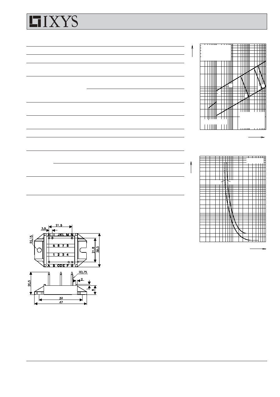
Fig. 1 Gate trigger characteristics
Fig. 2 Gate trigger delay time
Dimensions in mm (1 mm = 0.0394")