 | –≠–ª–µ–∫—Ç—Ä–æ–Ω–Ω—ã–π –∫–æ–º–ø–æ–Ω–µ–Ω—Ç: PDM4M4030 | –°–∫–∞—á–∞—Ç—å:  PDF PDF  ZIP ZIP |

Rev 2.2 - 7/17/97
8-25
1
2
3
4
5
6
7
8
9
10
11
12
Features:
n
High-density 2 megabit Static RAM module
n
Low profile 64-pin ZIP (Zig-zag In-line vertical
Package), 64-pin SIMM or Angled SIMM (Single
In-line Memory Module)
n
Ultra fast access time: 10 ns (max.)
n
Surface mounted plastic components on an epoxy
laminate (FR-4) substrate
n
Single 5V (
±
10%) power supply
n
Multiple V
SS
pins and decoupling capacitors for
maximum noise immunity
n
Inputs/outputs directly TTL compatible
Description:
The PDM4M4030 is a 64K x 32 static RAM module
constructed on an epoxy laminate (FR-4) substrate
using eight 64K x 4 static RAMs in plastic SOJ
packages. Availability of four chip select lines (one
for each of two RAMs) provides byte access.
Extremely fast speeds can be achieved due to the use
of 256K Static RAMs fabricated in Paradigm's high-
performance, high-reliability CMOS technology. The
PDM4M4030 is available with access times as fast as
10 ns with minimal power consumption.
The PDM4M4030 is packaged in a 64-pin FR-4 ZIP
(Zig-zag In-line vertical Package), a 64-pin SIMM or
Angled SIMM (Single In-line Memory Module). The
ZIP configuration allows 64 pins to be placed on a
package 3.65" long and 0.35" wide. At only 0.650"
high, this low-profile package is ideal for systems
with minimum board spacing. The SIMM configura-
tion allows use of edge mounted sockets to secure the
module.
All inputs and outputs of the PDM4M4030 are TTL
compatible and operate from a single 5V supply. Full
asynchronous circuitry requires no clock or refresh for
operation and provides equal access and cycle times
for ease of use.
Two identification pins (PD0 and PD1) are provided
for applications in which different density versions of
the module are used. In this way, the target system
can read the respective levels of PD0 and PD1 to
determine a 64K depth.
PDM4M4030
64K x 32 CMOS
Static RAM Module
Functional Block Diagram
I/O31-I/O0
8
8
8
8
CS
1
CS
2
CS
3
CS
4
16
2
ADDRESS
WE
OE
PD
64K x 32
RAM

PDM4M4030
8-26
Rev 2.2 - 7/17/97
Pin Configuration
(1)
NOTE:
1. Pins 2 and 3 (PD0 and PD1) are read by the
user to determine the density of the module.
If PD0 reads OPEN and PD1 reads V
SS
then
the module has a 64K depth.
Pin Assignment
Pin
Signal
I/O31-I/O0
Data Inputs/Outputs
A15-A0
Addresses
CS
4-
CS
1
Chip Selects
WE
Write Enable
OE
Output Enable
PD1-PD0
Depth Identification
V
CC
Power
V
SS
Ground
NC
No Connect
2
4
6
8
10
12
14
16
18
20
22
24
26
28
30
32
34
36
38
40
42
44
46
48
50
52
54
56
58
60
62
64
1
3
5
7
9
11
13
15
17
19
21
23
25
27
29
31
33
35
37
39
41
43
45
47
49
51
53
55
57
59
61
63
PD0
I/O0
I/O1
I/O2
I/O3
Vcc
A7
A8
A9
I/O4
I/O5
I/O6
I/O7
WE
A14
CS
1
CS
3
NC
Vss
I/O16
I/O17
I/O18
I/O19
A10
A11
A12
A13
I/O20
I/O21
I/O22
I/O23
Vss
Vss
PD1
I/O8
I/O9
I/O10
I/O11
A0
A1
A2
I/O12
I/O13
I/O14
I/O15
Vss
A15
CS
2
CS
4
NC
OE
I/O24
I/O25
I/O26
I/O27
A3
A4
A5
Vcc
A6
I/O28
I/O29
I/O30
I/O31
ZIP, SIMM
TOP VIEW
PD0 - OPEN
PD1 - Vss
PDM4M4030
Rev 2.2 - 7/17/97
8-27
1
2
3
4
5
6
7
8
9
10
11
12
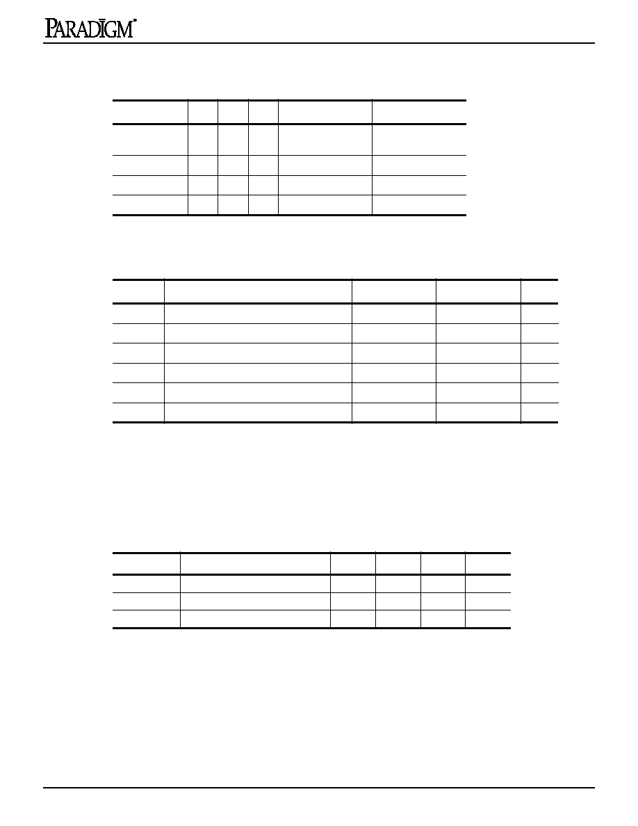
Recommended DC Operating Conditions
Symbol
Parameter
Min.
Typ.
Max.
Unit
V
CC
Supply Voltage
4.75
5.0
5.25
V
V
SS
Supply Voltage
0
0
0
V
Commercial
Ambient Temperature
0
25
70
∞
C
Absolute Maximum Ratings
(1)
NOTE:
1. Stresses greater than those listed under ABSOLUTE MAXIMUM RATINGS may cause permanent
damage to the device. This is a stress rating only and functional operation of the device at these or
any other conditions above those indicated in the operational sections of this specification is not
implied. Exposure to absolute maximum rating conditions for extended periods may affect
reliability.
Symbol
Rating
Com'l.
Ind.
Unit
V
TERM
Terminal Voltage with Respect to V
SS
≠0.5 to +7.0
≠0.5 to +7.0
V
T
BIAS
Temperature Under Bias
≠10 to +85
≠10 to +85
∞
C
T
STG
Storage Temperature
≠55 to +125
≠65 to +150
∞
C
T
A
Operating Temperature
0 to +70
0 to +70
∞
C
P
T
Power Dissipation
1.0
1.0
W
I
OUT
DC Output Current
50
50
mA
Truth Table
Mode
CS
OE
WE
Output
Power
Deselect/
Power-down
H
X
X
High-Z
Standby
Read
L
L
H
DATA
OUT
Active
Write
L
X
L
DATA
IN
Active
Deselect
L
H
H
High-Z
Active
PDM4M4030
8-28
Rev 2.2 - 7/17/97
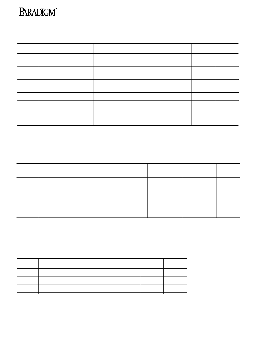
DC Electrical Characteristics
(V
CC
= 5.0V
±
5%, T
A
= 0
∞
C to 70
∞
C)
NOTE
1. V
IL
= ≠1.5V for pulse widths less than 10 ns, once per cycle.
2. I/O pins must not exceed V
CC
+ 0.5V.
Symbol
Parameter
Test Conditions
Min.
Max.
Unit
I
LI
Input Leakage Current
(Address)
V
CC
= Max.,V
IN
= V
SS
to V
CC
--
80
µ
A
I
LI
Input Leakage Current
(Data)
V
CC
= Max., V
IN
= V
SS
to V
CC
--
10
µ
A
I
LO
Output Leakage Current
V
OUT
= V
SS
to V
CC
, V
CC
= Max.,
CS
= V
IH
--
10
µ
A
V
OL
Output Low Voltage
I
OL
= 8 mA, V
CC
= Min.
--
0.4
V
V
OH
Output High Voltage
I
OL
= ≠4 mA, V
CC
= Min.
2.4
--
V
V
IH
(2)
Input High Voltage
2.2
6.0
V
V
IL
Input Low Voltage
≠0.5
(1)
0.8
V
Power Supply Characteristics
NOTE
1. Preliminary specification only.
Symbol
Parameter
10 ns - 15 ns
(1)
Max
20 ns - 25 ns
(1)
Max
Unit
I
CC
Operating Current
CS
= V
IL
, V
CC
= Max., f = f
MAX
, Outputs Open
1280
1280
mA
I
SB
Standby Current
CS
V
IH
, V
CC
= Max., f = f
MAX
, Outputs Open
320
320
mA
I
SB1
Full Standby Current
CS
V
CC
≠ 0.2V,
f = 0, V
IN
> V
CC
≠ 0.2V or < 0.2V
240
240
mA
Capacitance
(1)
(T
A
= +25
∞
C, f = 1.0 MHz)
NOTE
1. This parameter is determined by device characteristics but is not production tested.
Symbol Parameter
Max.
Unit
C
IN(D)
Input Capacitance, (Data) V
IN
= 0V
15
pF
C
IN(A)
Input Capacitance, (Address and Control) V
IN
= 0V
70
pF
C
OUT
Output Capacitance, V
OUT
= 0V
15
pF

PDM4M4030
Rev 2.2 - 7/17/97
8-29
1
2
3
4
5
6
7
8
9
10
11
12
AC Test Conditions
Input Pulse Levels
V
SS
to 3.0V
Input Rise/Fall Times
5 ns
Input Timing Reference Levels
1.5V
Output Reference Levels
1.5V
Output Load
See Figures 1 , 2
255
480
30 pF*
+5V
DATA
OUT
* Including scope and jig capacitances
Figure 1. Output Load
255
480
5 pF*
+5V
DATA
OUT
* Including scope and jig capacitances
Figure 2. Output Load
(for t
OHZ
, t
CHZ
, t
OLZ
, and t
CLZ
)
PDM4M4030
8-30
Rev 2.2 - 7/17/97
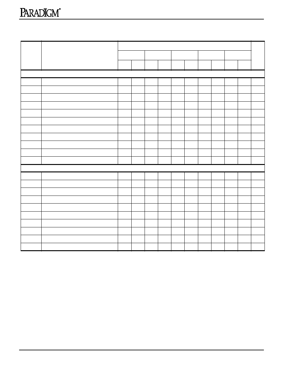
AC Electrical Characteristics
(Vcc = 5V
±
5%, T
A
= 0
∞
C to +70
∞
C)
NOTES 1. This parameter is determined by device characteristics but is not production tested.
2. Preliminary specifications only.
Symbol
Parameter
PDM4M4030SXXZ, PDM4M4030SXXM
Unit
-10 ns
(2)
-12 ns
(2)
-15 ns
(2)
-20 ns
-25 ns
Min.
Max.
Min.
Max.
Min.
Max.
Min.
Max.
Min.
Max.
Read Cycle
t
RC
Read Cycle Time
10
--
12
--
15
--
20
--
25
--
ns
t
AA
Address Access Time
--
10
--
12
--
15
--
20
--
25
ns
t
ACS
Chip Select Access Time
--
10
--
12
--
15
--
20
--
25
ns
t
CLZ
(1)
Chip Select to Output in Low-Z
2
--
2
--
2
--
3
--
3
--
ns
t
OE
Output Enable to Output Valid
--
5
--
7
--
9
--
10
--
12
ns
t
OLZ
(1)
Output Enable to Output in Low-Z
0
--
0
--
0
--
0
--
0
--
ns
t
CHZ
(1)
Chip Deselect to Output in High-Z
--
5
--
7
--
8
--
10
--
15
ns
t
OHZ
(1)
Output Disable to Output in High-Z
--
5
--
7
--
8
--
10
--
15
ns
t
OH
Output Hold from Address Change
3
--
3
--
3
--
3
--
3
--
ns
t
PU
(1)
Chip Select to Power Up Time
0
--
0
--
0
--
0
--
0
--
ns
t
PD
(1)
Chip Deselect to Power Up Time
--
10
--
12
--
15
--
20
--
25
ns
Write Cycle
t
WC
Write Cycle Time
10
--
12
--
15
--
20
--
25
--
ns
t
CW
Chip Select to End of Write
8
--
10
--
12
--
15
--
20
--
ns
t
AW
Address Valid to End of Write
9
--
11
--
13
--
15
--
20
--
ns
t
AS
Address Setup Time
1
≠
1
≠
1
≠
0
≠
0
--
ns
t
WP
Write Pulse Width
8
--
10
--
12
--
15
--
20
--
ns
t
WR
Write Recovery Time
0
--
0
--
0
--
0
--
0
--
ns
t
WHZ
(1)
Write Enable to Output in High-Z
--
5
--
7
--
8
--
12
--
15
ns
t
DW
Data to Write Time Overlap
5
--
7
--
8
--
12
--
15
--
ns
t
DH
Data Hold from Write Time
1
--
1
--
1
--
0
--
0
--
ns
t
OW
(1)
Output Active from End of Write
2
--
2
--
2
--
0
--
0
--
ns

PDM4M4030
Rev 2.2 - 7/17/97
8-31
1
2
3
4
5
6
7
8
9
10
11
12
Timing Waveforms of Read Cycle No.1
(1)
Timing Waveforms of Read Cycle No.2
(1,2,4)
Timing Waveforms of Read Cycle No.3
(1,3,4)
NOTES 1
WE
is HIGH for Read Cycle.
2. Device is continuously selected.
CS
= V
IL
.
3. Address valid prior to or coincident with
CS
transition LOW.
4.
OE
= V
IL
.
5. Transition is measured
±
200 mV for steady state. This parameter is
determined by device characteristics but is not production tested.
t
AA
t
RC
ADDRESS
t
OE
D
OUT
t
OH
t
CHZ(5)
t
OHZ(5)
t
ACS
t
CLZ(5)
CS
OE
t
OLZ(5)
t
AA
t
RC
ADDRESS
D
OUT
t
OH
t
OH
Previous Data Valid
Data Valid
t
ACS
CS
D
OUT
t
CLZ(5)
t
CLZ(5)

PDM4M4030
8-32
Rev 2.2 - 7/17/97
Timing Waveforms of Write Cycle No.1 (
WE
Controlled)
(1,2,3,7)
Timing Waveforms of Write Cycle No.2 (
CS
Controlled)
(1,2,3,5)
NOTES 1
WE
or
CS
must be HIGH during all address transitions.
2. A write occurs during the overlap (t
WP
) of a LOW
CS
and a LOW
WE
.
3. t
WR
is measured from the earlier of
CS
or
WE
going HIGH to end the write cycle.
4. During this period, I/O pins are in the output state, and input signals must be applied.
5. If the
CS
LOW transition occurs simultaneously with or after the
WE
LOW transition, the outputs
remain in a high-impedance state.
6. Transition is measured
±
200 mV for steady state with a 5 pF load (including scope and jig). This
parameter is determined by device characteristics but is not production tested.
7. If
OE
is LOW during a
WE
controlled write cycle, the write pulse width must be the larger of t
WP
or
(t
WHZ
+ t
DW
) to allow the I/O drivers to turn off and data to be placed on the bus for the required t
DW
.
If
OE
is HIGH during a
WE
controlled write cycle, this requirement does not apply and the write
pulse width can be as short as the specified t
WP
.
t
AW
CS
t
AS
t
WR
t
WC
t
CW
t
DH
t
DW
D
IN
WE
ADDRESS
Data Valid
t
AW
CS
D
OUT
t
AS
t
WR
t
WC
t
WP(7)
t
WHZ(6)
t
OHZ(6)
t
OW(6)
t
OHZ (6)
t
DH
t
DW
D
IN
WE
OE
ADDRESS
Data Valid
(4)
(4)

PDM4M4030
Rev 2.2 - 7/17/97
8-33
1
2
3
4
5
6
7
8
9
10
11
12
Package Dimensions
SIMM Version
ZIP Version
3.650
0.500
0.120
0.150
PIN 1
FRONT VIEW
COMPONENTS THIS SIDE
(NOT SHOWN)
COMPONENTS THIS SIDE
(NOT SHOWN)
0.350
0.100
SIDE VIEW
0.050
0.100
0.020
0.250
BACK VIEW
PIN 1
0.135
0.165
3.850
0.630
PIN 1
FRONT VIEW
COMPONENTS THIS SIDE
(NOTE SHOWN)
COMPONENTS THIS SIDE
(NOTE SHOWN)
BACK VIEW
0.350
0.050
SIDE VIEW
0.250
0.050
0.400
3.584
0.250
PIN 1

PDM4M4030
8-34
Rev 2.2 - 7/17/97
3.855
3.845
PIN 1
COMPONENTS BOTH SIDES
(NOT SHOWN)
0.330
Max.
SIDE VIEW
0.255
0.245
0.630 R
0.610 R
0.050
Typical
0.403
0.397
3.588
3.580
3.552
3.548
0.251
0.249
0.085
0.075
0.255
0.245
0.600
0.590
Ordering Information
PDM4M XXXXX S XX X X
Device Power Speed Package Temp
Blank
Commercial (0 to 70
∞
C)
Z
AM
M
64-pin ZIP
64-pin Angled SIMM
64-pin SIMM
10
12
15
20
25
Commercial
S
Standard Power
4030
64K x 32
Angled SIMM Version