IXYS Corporation
3540 Bassett Street, Santa Clara,CA 95054
Tel: 408-982-0700 Fax: 408-496-0670
IXYS Semiconductor
Edisonstr. 15, D-68623 Lampertheim, Germany
Tel: +49-6206-5030 Fax: +49-6206-503629
I
XYS reserves the right to change limits, test conditions, and dimensions.
Symbol
Test Conditions
Maximum Ratings
V
DSS
T
J
= 25
∞
C to 150∞C
200
V
V
DGR
T
J
= 25
∞
C to 150∞C; R
GS
= 10 k
200
V
V
G S
Continuous
±
20
V
V
GSM
Transient
±
30
V
I
D25
T
K
= 25
∞
C
418
A
I
DM
T
K
= 25
∞
C, t
P
= 10
µ
s
1672
A
P
D
T
C
= 25
∞
C
2450
W
T
K
= 25
∞
C
1640
W
T
J
-40 ...+150
∞
C
T
JM
150
∞
C
T
stg
-40 ... +125
∞
C
V
ISOL
50/60 Hz
t = 1 min
3000
V~
I
ISOL
1 mA
t = 1 s
3600
V~
M
d
Mounting torque (M6)
2.25-2.75/20-25 Nm/lb.in.
Terminal connection torque (M5)
2.5-3.7/22-33 Nm/lb.in.
Weight
typical including screws
250
g
Symbol
Test Conditions
Characteristic Values
(T
J
= 25
∞
C, unless otherwise specified)
min.
typ.
max.
V
DSS
V
GS
= 0 V, I
D
= 12 mA
200
V
V
GS(th)
V
DS
= 20 V, I
D
= 120 mA
3
6
V
I
GSS
V
GS
=
±
20 V DC, V
DS
= 0
±
500
nA
I
DSS
V
DS
= V
DSS
,
V
GS
= 0 V
T
J
= 25
∞
C
2.5 mA
V
DS
= 0.8 ∑ V
DSS
,
V
GS
= 0 V
T
J
= 125
∞
C
12 mA
R
DS(on)
V
GS
= 10 V, I
D
= 0.5 ∑ I
D25
4.2 m
Pulse test, t
300
µ
s, duty cycle d
2 %
1
2
11
10
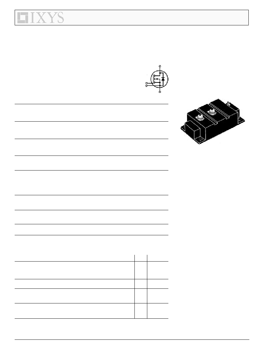
MegaMOS
TM
FET
VMO 400-02F
V
DSS
= 200 V
Module
I
D25
= 418 A
R
DS(on)
= 4.2 m
N-Channel Enhancement Mode
1 = Drain
2 = Source
10 = Kelvin Source
11 = Gate
1
2
10
11
Features
q
International standard package
q
Direct Copper Bonded Al
2
O
3
ceramic
base plate
q
Isolation voltage 3600 V~
q
Low R
DS(on)
HDMOS
TM
process
q
Low package inductance for high
speed switching
q
Kelvin Source contact for easy drive
Applications
q
AC motor speed control for electric
vehicles
q
DC servo and robot drives
q
Switched-mode and resonant-mode
power supplies
q
DC choppers
Advantages
q
Easy to mount
q
Space and weight savings
q
High power density
q
Low losses

IXYS MOSFETS and IGBTs are covered by one or more of the following U.S. patents:
4,835,592
4,881,106
5,017,508
5,049,961 5,187,117 5,486,715
4,850,072
4,931,844
5,034,796
5,063,307 5,237,481 5,381,025
VMO 400-02F
Symbol
Test Conditions
Characteristic Values
(T
J
= 25
∞
C, unless otherwise specified)
min.
typ.
max.
g
fs
V
DS
= 10 V; I
D
= 0.5 ∑ I
D25
pulsed
380
S
C
iss
53
nF
C
oss
V
GS
= 0 V, V
DS
= 25 V, f = 1 MHz
9.6
nF
C
rss
3.4
nF
t
d(on)
210
ns
t
r
V
GS
= 10 V, V
DS
= 0.5 ∑ V
DSS
, I
D
= 0.5 ∑ I
D25
500
ns
t
d(off)
R
G
= 1
(External)
900
ns
t
f
350
ns
Q
g
2300
nC
Q
gs
V
GS
= 10 V, V
DS
= 0.5 ∑ V
DSS
, I
D
= 0.5 ∑ I
D25
420
nC
Q
gd
1150
nC
R
thJC
0.051 K/W
R
thJK
with 30
µ
m heat transfer paste
0.076 K/W
Source-Drain Diode
Characteristic Values
(T
J
= 25
∞
C, unless otherwise specified)
Symbol
Test Conditions
min.
typ.
max.
I
S
V
GS
= 0 V
418
A
I
SM
Repetitive; pulse width limited by T
JM
1672
A
V
SD
I
F
= I
S
; V
GS
= 0 V,
0.9
1.2
V
Pulse test, t
300
µ
s, duty cycle d
2 %
t
rr
I
F
= I
S
, -di/dt = 1200 A/
µ
s, V
DS
= 100 V
600
ns
Dimensions in mm (1 mm = 0.0394")
IXYS Corporation
3540 Bassett Street, Santa Clara,CA 95054
Tel: 408-982-0700 Fax: 408-496-0670
IXYS Semiconductor
Edisonstr. 15, D-68623 Lampertheim, Germany
Tel: +49-6206-5030 Fax: +49-6206-503629
I
XYS reserves the right to change limits, test conditions, and dimensions.
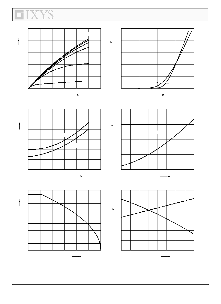
VMO 400-02F
Fig. 1 Typical output characteristics I
D
= f (V
DS
)
Fig. 2 Typical transfer characteristics I
D
= f (V
GS
)
0
1
2
3
4
5
6
0
250
500
750
1000
1250
5 V
6 V
7 V
8 V
9 V
V
DS
I
D
A
V
A
I
D
0
2
4
6
8
0
250
500
750
1000
1250
V
DS
= 30 V
V
V
GS
T
J
= 125∞C
T
J
= 25∞C
0
25
50
75
100
125
150
0
50
100
150
200
250
300
350
400
450
T
S
T
J
∞C
A
-50
-25
0
25
50
75
100
125
150
0,6
0,7
0,8
0,9
1,0
1,1
1,2
V
DSS
norm.
∞C
V
GS(th)
-50
-25
0
25
50
75
100
125
150
0,5
1,0
1,5
2,0
2,5
norm.
∞C
0
200
400
600
800
1000
1200
0,8
0,9
1,0
1,1
1,2
1,3
1,4
R
DS(on)
T
J
V
GS
= 15 V
V
DSS
V
GS
= 10 V
A
I
D
norm.
R
DS(on)
I
D
V
GS
= 10 V
V
GS(th)
I
D
= 210 A
Fig. 5 Continuous drain current I
D
= f (T
K
)
Fig. 6 V
DSS
= f (T
J
), V
GS(th)
= f (T
J
), normalized
Fig. 3 Typical R
DS(on)
= f (I
D
), normalized
Fig. 4 R
DS(on)
= f (T
J
), normalized
IXYS MOSFETS and IGBTs are covered by one or more of the following U.S. patents:
4,835,592
4,881,106
5,017,508
5,049,961 5,187,117 5,486,715
4,850,072
4,931,844
5,034,796
5,063,307 5,237,481 5,381,025
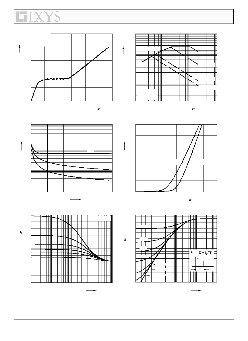
VMO 400-02F
0.001
0.01
0.1
1
10
0.001
0.01
0.1
1
10
100
1000
1
10
100
1000
10000
Z
thJK
D=0.01
D=0.02
D=0.05
D= 0.1
D= 0.2
D = 0.5
s
K/W
0
500
1000
1500
2000
2500
3000
0
3
6
9
12
15
V
GS
V
I
D
A
Limited by R
DS(on)
t = 100 ms
t = 10 ms
V
DS
V
0.0001
0.001
0.01
0.1
1
0
100
200
300
400
500
600
700
800
900
1000
t
t
p
s
0.00
0.25
0.50
0.75
1.00
1.25
1.50
0
200
400
600
800
1000
1200
T
J
= 25∞C
T
J
= 125∞C
V
A
0
5
10
15
20
25
1
10
100
1000
nF
V
SD
I
S
C
oss
V
DS
V
C
I
D
= 210 A
I
G
= 12 mA
V
DS
= 100 V
Q
g
nC
t = 1 ms
non-repetitive
T
J
= 150∞C
T
S
= 25∞C
C
iss
C
rss
I
d
A
D = single pulse
0
DC operation
D= 0.1
D= 0.2
D= 0.3
D= 0.4
D= 0.5
D= 0.7
T
K
= 80
∞
C
Fig. 7 Typical turn-on gate charge characteristics
Fig. 8 Forward Bias Safe Operating Area, I
D
= f (V
DS
)
p
Fig. 11 Drain current versus pulse width and
Fig. 12 Transient thermal resistance Z
thJK
= f (t
p
)
duty cycle
Fig. 9 Typical capacitances C = f (V
DS
), f = 1 MHz
Fig. 10 Typical forward characteristics of reverse
diode, I
S
= f (V
SD
)