 | –≠–ª–µ–∫—Ç—Ä–æ–Ω–Ω—ã–π –∫–æ–º–ø–æ–Ω–µ–Ω—Ç: KLI-8811 | –°–∫–∞—á–∞—Ç—å:  PDF PDF  ZIP ZIP |

Eastman Kodak Company ≠ Image Sensor Solutions - Rochester, NY 14650-2010
Phone (716) 722-4385 Fax (716) 477-4947
Web: www.kodak.com/go/ccd E-mail: ccd@kodak.com
KLI-8811
KLI-8811
8800 Element Linear CCD Image Sensor
Performance Specification
Eastman Kodak Company
Image Sensor Solutions
Rochester, New York 14650-2010
Revision 0
October 3, 2000

Eastman Kodak Company ≠ Image Sensor Solutions - Rochester, NY 14650-2010
Phone (716) 722-4385 Fax (716) 477-4947
Web: www.kodak.com/go/ccd E-mail: ccd@kodak.com
2
Revision. 0
KLI-8811
TABLE OF CONTENTS
1.1
Features---------------------------------------------------------------------------------------------------------3
1.2
Description -----------------------------------------------------------------------------------------------------3
1.3
Imaging ---------------------------------------------------------------------------------------------------------5
1.4
User-Selectable Resolution ----------------------------------------------------------------------------------5
1.5
Charge Transport and Sensing ------------------------------------------------------------------------------5
2.1
Package Configurations --------------------------------------------------------------------------------------6
2.2
Pin Description ------------------------------------------------------------------------------------------------8
2.3
Maximum Ratings --------------------------------------------------------------------------------------------9
2.4
DC Conditions----------------------------------------------------------------------------------------------- 10
2.5
AC Clock Level Conditions ------------------------------------------------------------------------------- 11
2.6
Clock Line Capacitance ------------------------------------------------------------------------------------ 11
2.7
AC Timing --------------------------------------------------------------------------------------------------- 12
2.7.1 Timing Diagram--------------------------------------------------------------------------------------------- 13
3.1
Image Specifications---------------------------------------------------------------------------------------- 14
3.1.1 Device Responsivity ---------------------------------------------------------------------------------------- 15
3.2
Defect Classification---------------------------------------------------------------------------------------- 15
4.1
Quality Assurance and Reliability ------------------------------------------------------------------------ 16
4.2
Ordering Information --------------------------------------------------------------------------------------- 16
FIGURES
Figure 1
Single Channel Schematic -----------------------------------------------------------------------------3
Figure 2
Functional Block Diagram -----------------------------------------------------------------------------4
Figure 3
Packaging Configuration ≠ Cerdip Package ---------------------------------------------------------6
Figure 4
Packaging Configuration ≠ Ceramic/Copper/Tungsten Package ---------------------------------7
Figure 5
ESD Protection Circuit ---------------------------------------------------------------------------------9
Figure 6
Typical Output Bias/Buffer Circuit ----------------------------------------------------------------- 10
Figure 7
Output Waveforms ------------------------------------------------------------------------------------ 12
Figure 8
Typical Responsivity---------------------------------------------------------------------------------- 15

Eastman Kodak Company ≠ Image Sensor Solutions - Rochester, NY 14650-2010
Phone (716) 722-4385 Fax (716) 477-4947
Web: www.kodak.com/go/ccd E-mail: ccd@kodak.com
3
Revision. 0
KLI-8811
1.1
Features
∑
User Selectable High Resolution:
8800 or 7300 active pixels
∑
High Sensitivity
∑
Wide Dynamic Range
∑
No Image Lag
∑
High Charge Transfer Efficiency
∑
Up to 1.4V peak-peak Output
∑
Two-Phase Register Clocking
∑
On-chip Dark Reference
∑
30MHz per channel with Copper/Tungsten
package configuration. (120Mhz data rate)
1.2
Description
The KLI-8811 is a linear imaging Charge-Coupled Device
(CCD) designed for high resolution scanning applications.
Each device contains a row of 8800 active photoelements,
consisting of high performance pinned diodes for
improved sensitivity, lower noise and the elimination of
lag. Readout of the pixel data
is accomplished through the use of four CCD shift
registers, positioned on each side of the photodiode array
and divided into left and right halves that read towards the
center of the device. The photodiodes are 7µm x 7µm and
are located on 7µm centers. The array is structured so as
to provide 8 'blank' CCD cells followed by 2200 pixels of
active image data for each output. 10 dark reference pixels
follow the active pixels, then 4 test pixels, followed by 2
'blank' CCD cells for each output. The user has the option
of reducing the resolution to 7300 active pixels by
draining the remainder of the charge packets from the shift
registers using the resolution select control gate. The
devices are manufactured using NMOS, buried channel
processing and utilize dual layer polysilicon and dual
layer metal technologies. The die size is 63.5 mm X 1.2
mm and is housed in dual-in-line packages in either
0.600" wide, 40-pin cerdip package (see Figure 3), or,
0.400
wide, cofired ceramic package with a copper-
tungsten heat sink (see Figure 4) configurations. The
cover glass is Corning 7059 with multi-layer anti-
reflective (MAR) coatings.
2200 Active Pixels
Drain
RS
Phi1
Phi2
TG
IG
ID
VRD
PhiR
VDD
VID
SUB
OG
10 Dark
4 Test
2 blank
CCD
cells
8
blank
CCD
cells
Figure 1 - Single Channel Schematic
Eastman Kodak Company ≠ Image Sensor Solutions - Rochester, NY 14650-2010
Phone (716) 722-4385 Fax (716) 477-4947
Web: www.kodak.com/go/ccd E-mail: ccd@kodak.com
4
Revision 0
KLI-8811
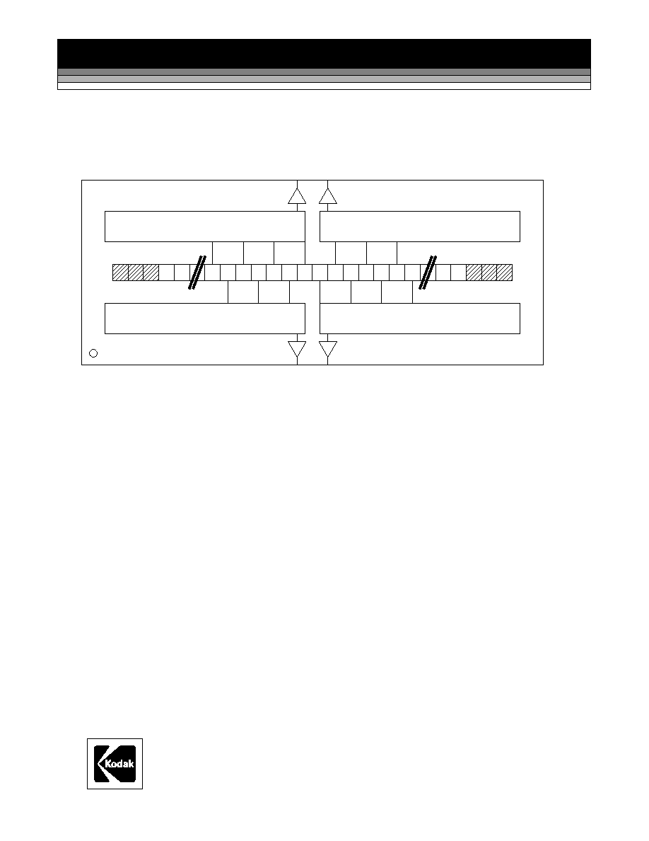
Figure 2 - Functional Block Diagram
D Channel
B Channel Output
1st active pixel is # 4402
Last active pixel is # 8800
D Channel Output
1st active pixel is # 4400
Last active pixel is # 2
A Channel Output
1st active pixel is # 4401
Last active pixel is # 8799
C Channel Output
1st active pixel is # 4399
Last active pixel is # 1
Pin #1
corner
B Channel
C Channel
A Channel
1
8800

Eastman Kodak Company ≠ Image Sensor Solutions - Rochester, NY 14650-2010
Phone (716) 722-4385 Fax (716) 477-4947
Web: www.kodak.com/go/ccd E-mail: ccd@kodak.com
5
Revision 0
KLI-8811
1.3
Imaging
During the integration period, an image is obtained by
gathering electrons generated by photons incident upon
the photodiodes. The charge collected in the photodiode
array is a linear function of the local exposure. Storage
of the charge carriers occurs adjacent to the photodiode
in the accumulation phase that is self-biased on-chip.
Isolation from the CCD shift registers during the
integration period is provided by the transfer gate TG,
which is held 'off' at a barrier potential. At the end of the
integration period, the CCD register clocking is stopped
and the H1 shift register clock is turned 'on'. Next, the
transfer gate TG is turned 'on' causing the charge to drain
from the accumulation phase, through the TG region and
into the H1 storage region. Once the transfer is complete,
TG is turned 'off' once again to isolate the two regions.
Complementary clocking of the H1 and H2 phases
subsequently resumes for the readout of the current line
of data while the next line of data is integrated.
1.4
User-Selectable Resolution
The CCD shift registers are outfitted with a resolution
select feature. This feature consists of two control gates
labeled RS and H2x. The control gates allow the user to
select the high-resolution mode (8800 pixels), or low
resolution mode (7300 pixels).
When the RS pin is held at a low potential, (0V), and
H2x is connected to H2, the imager will be in the high-
resolution mode utilizing all 8800 active pixels.
When the RS pin is held at a high potential, (15V), and
H2x is biased to a low potential, (0V), all the charge
packets that are clocked into the CCD phase adjacent to
the control gate will be emptied of charge carriers. The
low resolution mode has the advantage of allowing the
clocks to be stopped after the 7300 pixels have been
read-out and the next integration period started, thus
reducing the line integration time.
1.5
Charge Transport and Sensing
Readout of the signal charge is accomplished by two-
phase, complementary clocking of the H1 and H2 gates.
The data in all registers is clocked simultaneously toward
the output structures. The signal is then transferred to the
output structures in a parallel format at the falling edge
of the H2 clock. The first active pixel data is available on
the ninth H2 falling-edge after the transfer period. Re-
settable floating diffusions are used for the charge to
voltage conversion while source-followers provide
buffering to external connections. The potential change
on the floating diffusion is dependent on the amount of
signal charge and is given by
V
FD
=
Q/C
FD
. Prior to
each pixel output, the floating diffusion is returned to the
V
RD
level by the reset clock, PHLR. In order to reduce
on-chip power dissipation and provide optimum
linearity, an off-chip current sink for the third stage
source-follower is required for proper operation of the
device. (See Operating Conditions.)