www.latticesemi.com
1
ip1007_06
PCI Core Version 3
September 2004
IP Data Sheet
© 2004 Lattice Semiconductor Corp. All Lattice trademarks, registered trademarks, patents, and disclaimers are as listed at www.latticesemi.com/legal. All other brand
or product names are trademarks or registered trademarks of their respective holders. The specifications and information herein are subject to change without notice.
The product described herein is subject to continuing development, and applicable specifications and information are subject to change without notice. Such specifica-
tions and information are provided in good faith; actual performance is not guaranteed, as it is dependent on many factors, including the user's system design.
Features
Available as 32/64-Bit PCI Bus and 32/64-Bit
Local Bus
Available in Master/Target and Target
Versions
PCI SIG Local Bus Specification, Revision
2.2 Compliant
64-Bit Addressing Support
Capabilities List Pointer Support
Parity Error Detection
Up to Six Base Address Registers (BARs)
Expansion ROM BAR Support
Fast Back-to-Back Transaction Support
Supports Zero Wait State Transactions
Special Cycle Transaction Support
Customizable Configuration Space
Up to 66MHz PCI
Fully Synchronous Design
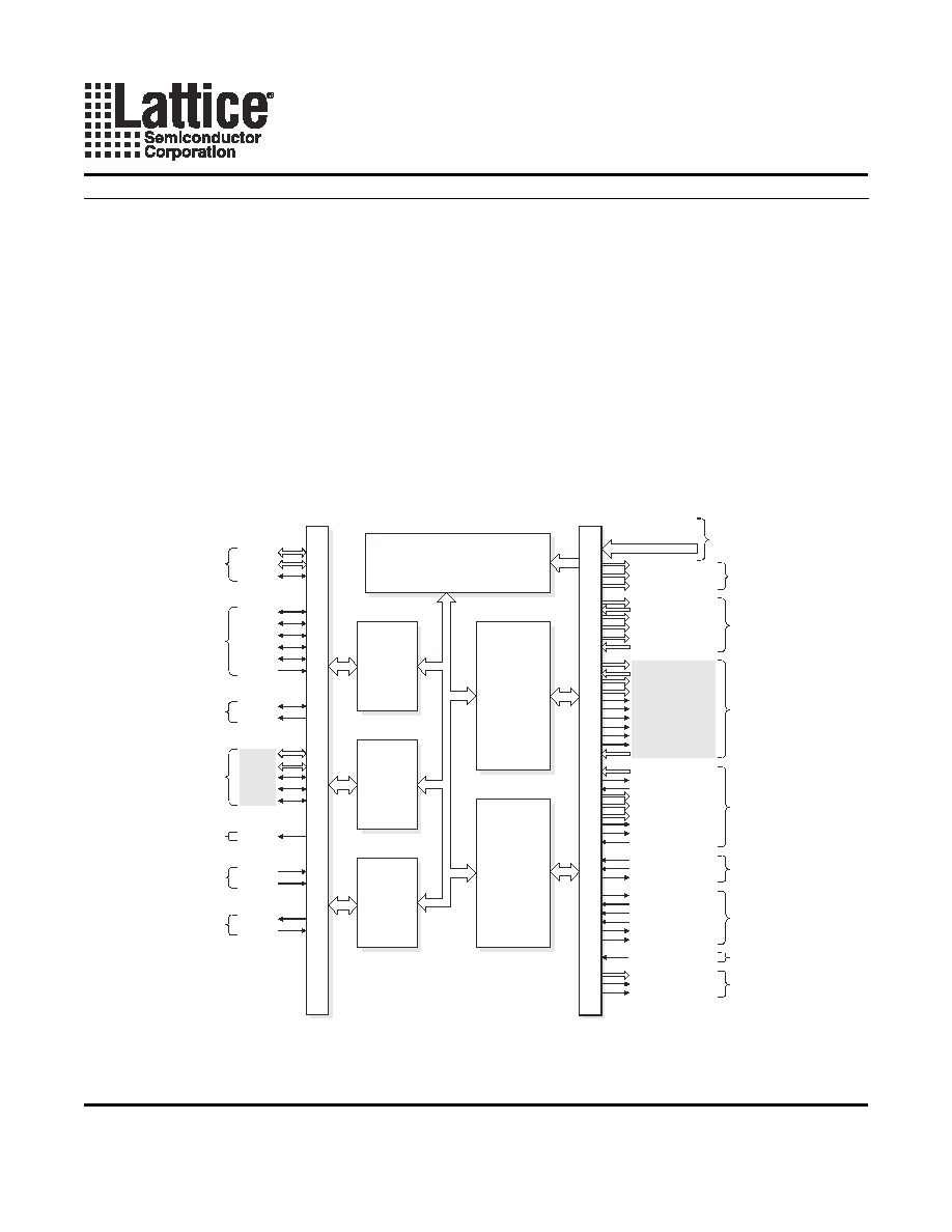
Block Diagram
PCI Master/Target Block Diagram
Note: Signals in shaded boxes are used for 64-bit PCI Cores.
Local
Target
Interface
Control
Configuration
Space
Parity
Generator
and
Checker
Local
Interface
cache[7:0]
l_Interruptn
command[9:0]
status[5:0]
intan
cben[3:0]
par
ad[31:0]
idsel
framen
trdyn
irdyn
stopn
devseln
rstn
clk
perrn
serrn
ad[63:32]
cben[7:4]
par64
req64n
ack64n
Address
& Data
Interface
Control
Error
Reporting
64-Bit
Extension
Interrupt
System
lt_command_out[3:0]
l_data_out[31:0]
l_ad_in[31:0]
lt_cben_out[3:0]
lt_address_out[31:0]
l_data_out[63:32]
l_ad_in[63:32]
lt_cben_out[7:4]
lt_address_out[63:32]
lt_disconnectn
lt_abortn
lt_rdyn
lt_r_nw
lt_64bit_transn
lt_ldata_xfern
lt_hdata_xfern
Config
Register
Address
& Data
64-Bit
Extension
Interrupt
Target
Interface
Control
Decode
exprom_hit
bar_hit[5:0]
lt_accessn
new_cap_hit
lm_req32n
lm_req64n
lm_rdyn
lm_burst_length[11:0]
lm_ldata_xfern
lm_hdata_xfern
lm_64bit_transn
lm_gntn
lm_status[3:0]
lm_termination[2:0]
lm_burst_cnt[12:0]
gntn
reqn
Arbitration
Master
Interface
Control
Master
req/gnt
lm_r_nw
lm_timeoutn
lm_abortn
lm_cben_in[7:4]
lm_cben_in[3:0]
lm_data_xfern
lt_data_xfern
PCI
Target
Control
PCI
Master
Control
Local
Master
Interface
Control
PCI
Interface
Configuration
space port
[401:0]

Lattice Semiconductor
PCI Core Version 3
2
General Description
Peripheral Component Interconnect (PCI) is a widely accepted bus standard that is used in many applications
including telecommunications, embedded systems, high performance peripheral cards, and networking.
Lattice's PCI core provides an ideal solution that meets the needs of today's high performance PCI applications. It
is fully compliant with the PCI Local Bus Specification, revision 2.2 for speeds up to 66MHz. The PCI core provides
a customizable 32/64-bit master/target or target solution. The core bridges the gap between the PCI interface and
a specific design application, providing an integrated PCI solution. The PCI solution allows designers to focus on
the application rather than on the PCI specification, resulting in a faster time-to-market.
The Lattice PCI offering is available in a number of configurations covering 32-bit PCI, 64-bit PCI, 32-bit local bus,
64-bit local bus, master/target and target applications. In this document, details of 64-bit operation and master
operation only apply when relevant. The appendix to this data sheet shows what cores are available on which
devices.
Functional Description
Figure 1 illustrates the functional blocks and bus structure used in the PCI core. The functional blocks are
described in more detail below.
PCI Master Control
The PCI master control interfaces with the PCI bus. It supports all of the address and control signals for generating
both the 32-bit and 64-bit data transactions on the PCI bus. For systems with address maps larger than four
gigabytes, the master generates dual address cycles (64-bit addressing). Table 1 shows a complete list of sup-
ported PCI commands that the master control can generate.
PCI Target Control
The PCI target control interfaces with the PCI bus. It supports all of the required address and command signals for
both the 32-bit and 64-bit PCI applications and additional signals including interrupts (
intan
). The PCI core also
supports 64-bit addressing (dual address cycles) for applications that require addressing memory spaces larger
than four gigabytes.
The PCI target controller supports two modes for data transfer. In burst mode, it can maintain a 512 Mbytes per
second transfer rate during burst transactions when operating at 66MHz with a 64-bit data bus. Additionally, for
slower application, single data phase transaction can also be easily implemented.
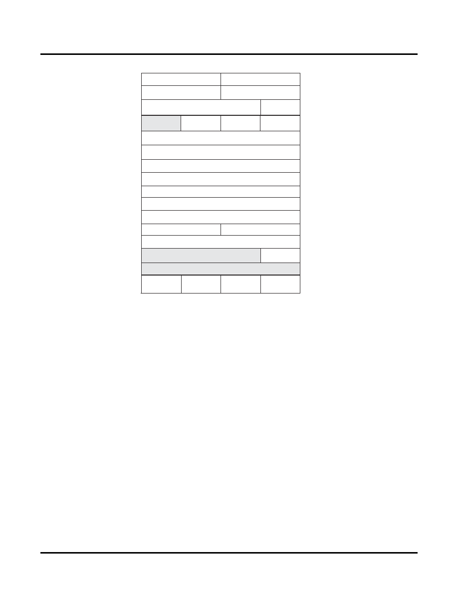
Table 1. Supported PCI Master/Target Commands
cben[3:0]
Command Type
Support
0000
Interrupt Acknowledge
Yes
0001
Special Cycle
Yes
0010
I/O Read
Yes
0011
I/O Write
Yes
0100
Reserved
Ignored
1
0101
Reserved
Ignored
1
0110
Memory Read
Yes
0111
Memory Write
Yes
1000
Reserved
Ignored
1
1001
Reserved
Ignored
1
1010
Configuration Read
Yes
1011
Configuration Write
Yes
1100
Memory Read Multiple
Yes

Lattice Semiconductor
PCI Core Version 3
3
Local Master Interface Control
The local master interface facilitates master transactions on the PCI Bus by generating the commands listed in
Table 1. The Local Master Interface Control passes the local transaction request to the PCI Master Control that
generates the PCI bus transaction. Latency control provides the local bus with the flexibility to efficiently interface to
the backend design.
Local Target Interface Control
The local target interface control responds to target transactions on the PCI bus. Fully decoded BAR select signals
(
bar_hit
), new capabilities select signal (
new_cap_hit
), and Expansion ROM BAR select signals
(
exprom_hit
) are provided by the Local Target Control to indicate that the PCI Core has been selected for a
transaction. Registered address and command signals are available at the local interface from the Local Interface
Control. Additionally, the local interface also supplies configuration bits and a local interrupt request
(
l_interruptn
).
Configuration Space
The configuration space implements all the necessary configuration space registers required to support the single
function PCI Master/Target. It provides the first 64 bytes of header type 0, which is used for all devices other than
PCI-to-PCI and CardBus bridges. Included in the 64 bytes are six Base Address Registers (BARs), the Expansion
ROM BAR, the Capabilities Pointer (
Cap pointer
), and registers that control the interrupt capability. The configu-
ration space also provides access to the
MIN_GNT
and
MAX_LAT
for the PCI Master interface. Figure 1 illustrates
the supported configuration space for the PCI core.
1101
Dual Address Cycle
Yes
1110
Memory Read Line
Yes
1111
Memory Write and Invalidate
Yes
1. Ignored bus cycles return "0"s.
Table 1. Supported PCI Master/Target Commands (Continued)
cben[3:0]
Command Type
Support
Lattice Semiconductor
PCI Core Version 3
4
Figure 1. PCI Core Configuration Space
Parity Generator and Checker
The parity generator and checker determines if the master is successful in addressing the desired target. It also
verifies that data transfers occur correctly between the master and target. The address and byte enable signals are
included in every calculation to ensure accuracy. Each address and data cycle that occurs on the PCI bus is
checked for errors. Every device writing addresses to
ad[31:0]
or
ad[63:32]
must also drive the
par
and
par64
signals.
Regardless of whether or not the address and byte enable signals carry any meaningful information, parity check-
ing is always performed. The parity checking signals
perrn
and
serrn
can be enabled or disabled through bit six
and bit eight of the PCI command register, included in the configuration space.
Local Bus Interface
Target Operation
Initially, the Local target is idle.
A valid transaction in the PCI bus is indicated to the local bus side by the assertion of
lt_accessn
signal. At this
time, either
bar_hit
,
new_cap_hit
or
exprom_hit
signal indicates which bar is selected and
lt_command_out
indicates the current PCI command type. If the command is "special cycle," then no BAR is
selected, otherwise the selected BAR needs to prepare the next process.
For a memory read command, the local target puts data on
lt_ad_in
and asserts
lt_rdyn
to indicate that the
data on
l_ad_in
is valid. The core will read the data and assert
lt_data_xfern
after
lt_rdyn
is active. When
Device ID
Vendor ID
00h
Status Register
Command Register
04h
Class Code
Revision
ID
08h
BIST
Header
Type
Latency
Timer
Cache
Line Size
0Ch
Base Address 0
10h
Base Address 1
14h
Base Address 2
18h
Base Address 3
1Ch
Base Address 4
20h
Base Address 5
24h
Cardbus CIS Pointer
28h
Subsystem ID
Subsystem Vendor ID
2Ch
Expansion ROM Base Address
30h
Reserved
Cap Ptr
34h
Reserved
38h
MAX_LAT
MIN_GNT
Interrupt
Pin
Interrupt
Line
3Ch
Note: Shaded sections indicate reserved and
unused sections in the configuration space. All
unused and reserved registers return 0s.

Lattice Semiconductor
PCI Core Version 3
5
the transaction is a burst read, the core will continue to keep asserting
lt_data_xfern
at subsequent clocks and
will read the data on
l_ad_in
if local side doesn't insert a wait cycle.
For a memory write command, the local target asserts
lt_rdyn
to indicate that it is ready to receive data on
l_data_out
. The core will write data on
l_data_out
and assert
lt_data_xfern
to indicate the data on
l_data_out valid
. The Local target will read the data on
l_data_out
.
When the local target bus width is 64-bit, the signals
lt_ldata_xfern
and
lt_hdata_xfern
are used together
instead of
lt_data_xfern
. For a 32-bit data width BAR, only
lt_ldata_xfern
is used. For a 64-bit data width
BAR,
lt_ldata_xfern
and
lt_hdata_xfern
are used together. The signal
lt_ldata_xfern
applies to the
lower 32-bits of data,
lt_hdata_xfern
applies to the upper 32 bits of data.
A target transaction is ended when
lt_accessn
becomes inactive. At this time,
bar_hit
,
new_cap_hit
and
exprom_hit
are all deasserted.
When a 32-bit BAR is hit, only the following local bus signals are used:
∑
l_ad_in[31:0]
,
l_data_out[31:0]
,
lt_cben_out[3:0]
and
lt_ldata_xfern
.
and the following signals are not used:
∑
l_ad_in[63:32]
,
l_data_out[63:32]
,
lt_cben_out[7:4]
and
lt_hdata_xfern
.
Master Operation
The Local master starts a transaction request by asserting
lm_req32n
or
lm_req64n
when
lm_status
is "Bus
Termination". At the same time, the local master needs to prepare the address, command and burst length on
l_ad_in
,
lm_cben_in[3:0]
and
lm_burst_length
respectively. Once the PCI bus grants the bus,
lm_gntn
is asserted to instruct the local master to continue with next process. Then the local master works with
lm_status
. A normal transaction status starts from "Bus Termination" to "Address Loading" to "Bus Transaction",
and ends with "Bus Termination". During "Bus Transaction", the local master reads or writes data based on the
lm_data_xfern
status which is similar to local target operation.
When the local master bus width is 64-bit,
lm_ldata_xfern
and
lm_hdata_xfern
are used instead of
lm_data_xfern
. For 32-bit data width BAR, only
lm_ldata_xfern
is used. For 64-bit data width BAR,
lm_ldata_xfern
and
lm_hdata_xfern
are used together. The signal
lm_ldata_xfern
applies to the lower
32 bits of data,
lm_hdata_xfern
applies to the upper 32 bits of data.

Lattice Semiconductor
PCI Core Version 3
6
Lattice PCI Core Configuration Options
The Lattice PCI Core allows an extensive definition of the PCI Configuration Space for optimum performance. Lat-
tice provides evaluation packages for both 32-bit and 64-bit PCI Bus sizes. For most other parameters, a set of sig-
nals called the Configuration Space Port is provided at the local bus side of the core to allow the user to define the
PCI configuration space as required for the user's system. Appropriate parameter values can be assigned to the
designated input signals of the Core Configuration Space Port in order to change the PCI configuration space to
meet your system's needs. There are two methods for configuring the parameters. These methods are fully
explained in the User's Guide for this IP Core. Please refer to the PCI Core User's Guide for a detailed description
of the parameters and methods for changing them.
Related Information
For more information regarding the verification and usage of the core, refer to the PCI Core User's Guide, available
on the Lattice web site at www.latticesemi.com.
For information regarding the PCI specification, refer to the PCI SIG, PCI Local Bus Specification, revision 2.2,
available on the PCI SIG web site at www.pcisig.com.
For other information, refer to PCI Hardware and Software Architecture and Design, written by Edward Solari and
George Willse.
The "PCI 2.2 Compliance Checklist" is available on the PCI SIG web site at www.pcisig.com.
Lattice Semiconductor
PCI Core Version 3
7
Appendix for LatticeECPTM and LatticeECTM FPGAs
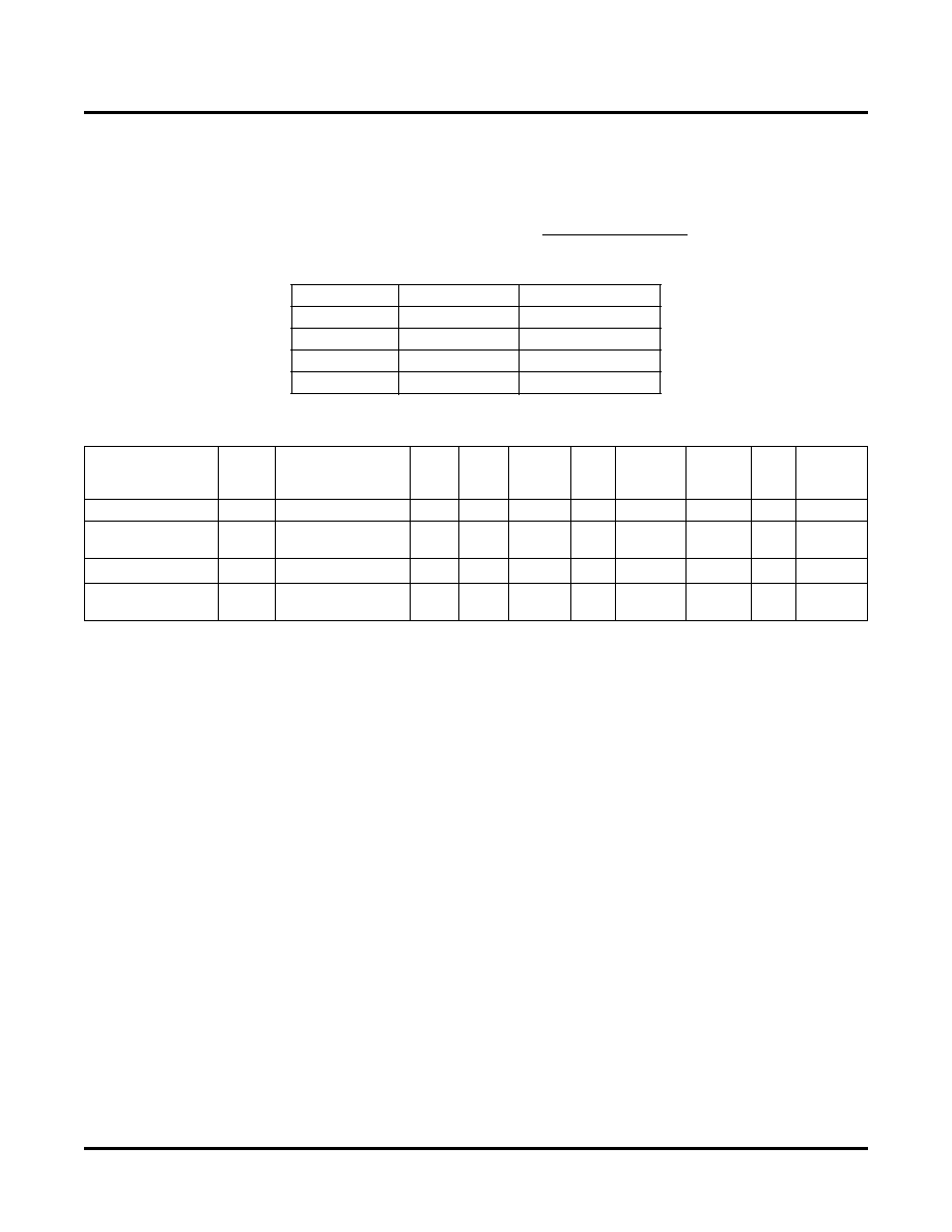
Supplied Netlist Configurations
The Ordering Part Number (OPN) for PCI cores on LatticeECP/EC devices varies by core type (Master/Target or
Target) and PCI Bus width (32-bit or 64-bit). Table 2 lists the available ordering part numbers. Table 3 lists the eval-
uation netlists that can be downloaded from the Lattice web site at www.latticesemi.com.
Table 2. Ordering Part Number (OPN) for PCI Core
Table 3. Performance and Resource Utilization
1
PCI Core on Other Lattice Devices
This PCI Core version 3 can be configured to work on other Lattice devices in addition to the ones shown here.
Please contact Lattice if you wish to use the PCI Core version 3 on a different Lattice device.
PCI Bus
Type
OPN
64-Bit
Master Target
PCI-MT64-E2-N3
64-Bit
Target
PCI-T64-E2-N3
32-Bit
Master Target
PCI-MT32-E2-N3
32-Bit
Target
PCI-T32-E2-N3
Configuration
Type
Device
PCI
Width
Local
Bus
Width SLICEs LUTs Registers
sysMEM
EBRs
f
MAX
(MHz)
External
Pins - PCI
Interface
pci_t32_e2_3_001 Target
LFEC20E-4F672C
2
32-bit
32-bit
467
729
445
0
33
48
pci_mt32_e2_3_001
Master/
Target
LFEC20E-4F672C
2
32-bit
32-bit
915
1548
625
0
33
49
pci_t64_e2_3_001 Target
LFEC20E-4F672C
2
64-bit
64-bit
667
1091
566
0
33
87
pci_mt64_e2_3_001
Master/
Target
LFEC20E-4F672C
2
64-bit
64-bit
1351
2361
819
0
33
89
1. Performance and utilization characteristics are generated using the stated device in Lattice's ispLEVER v.4.1 software. When using this IP
core in a different density, speed, or grade within the LatticeECP/EC family, performance may vary.
2. Configuration is for the devices indicated. Please contact your local Lattice sales representative if you wish to use another device.