 | ÐлекÑÑоннÑй компоненÑ: LT1217 | СкаÑаÑÑ:  PDF PDF  ZIP ZIP |
Äîêóìåíòàöèÿ è îïèñàíèÿ www.docs.chipfind.ru
1
LT1217
Low Power 10MHz
Current Feedback Amplifier
D
U
ESCRIPTIO
S
FEATURE
U
S
A
O
PPLICATI
The LT1217 is a 10MHz current feedback amplifier with DC
characteristics better than many voltage feedback ampli-
fiers. This versatile amplifier is fast, 280ns settling to 0.1%
for a 10V step thanks to its 500V/
µ
s slew rate. The LT1217
is manufactured on Linear Technology's proprietary
complementary bipolar process resulting in a low 1mA
quiescent current. To reduce power dissipation further,
the LT1217 can be turned off, eliminating the load current
and dropping the supply current to 350
µ
A.
The LT1217 is excellent for driving cables and other low
impedance loads thanks to a minimum output drive cur-
rent of 50mA. Operating on any supplies from
±
5V to
±
15V
allows the LT1217 to be used in almost any system. Like
other current feedback amplifiers, the LT1217 has high
gain bandwidth at high gains. The bandwidth is over 1MHz
at a gain of 100.
The LT1217 comes in the industry standard pinout and
can upgrade the performance of many older products.
s
1mA Quiescent Current
s
50mA Output Current (Minimum)
s
10MHz Bandwidth
s
500V/
µ
s Slew Rate
s
280ns Settling Time to 0.1%
s
Wide Supply Range,
±
5V to
±
15V
s
1mV Input Offset Voltage
s
100nA Input Bias Current
s
100M
Input Resistance
s
Video Amplifiers
s
Buffers
s
IF and RF Amplification
s
Cable Drivers
s
8, 10, 12-Bit Data Acquisition Systems
U
A
O
PPLICATI
TYPICAL
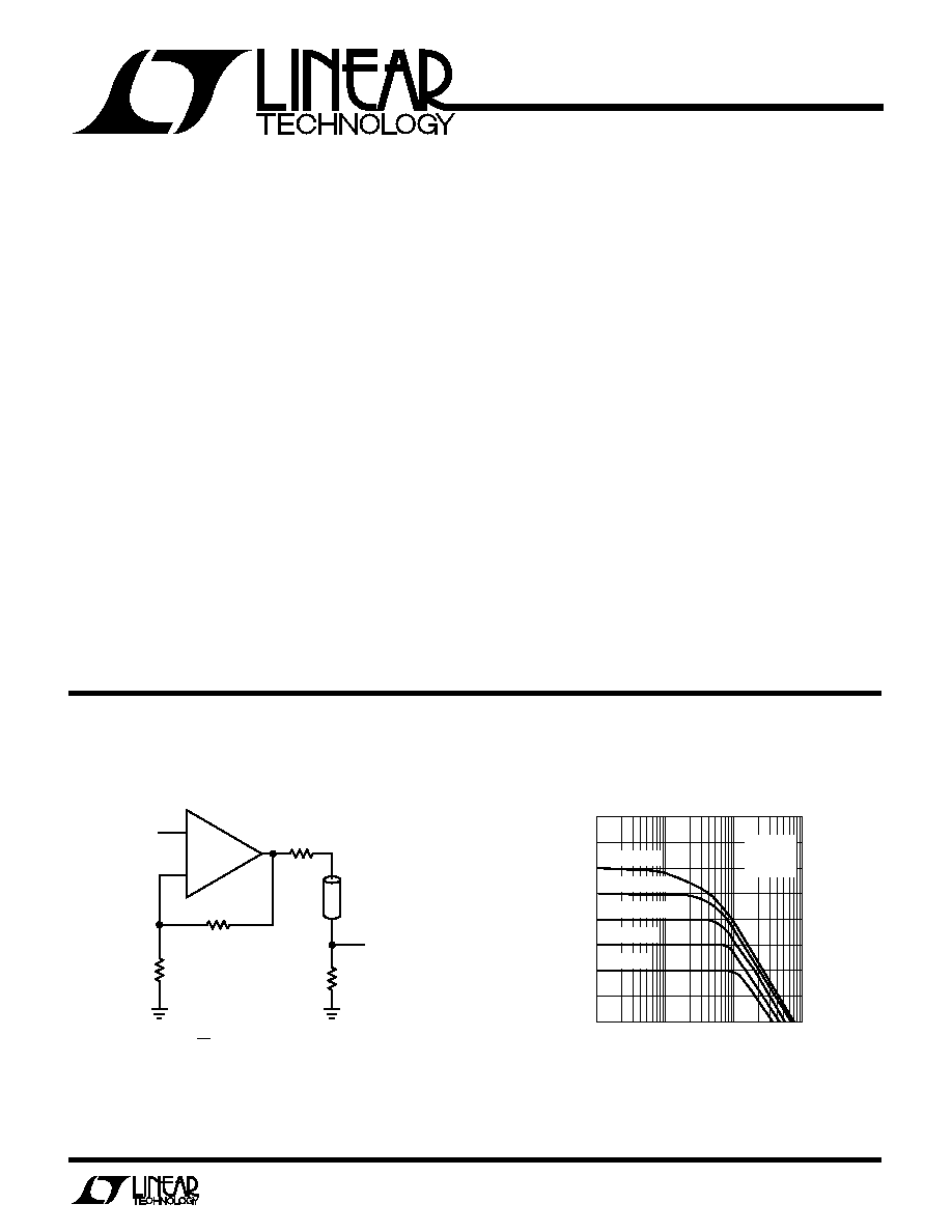
Cable Driver
Voltage Gain vs Frequency
FREQUENCY (Hz)
100k
20
AMPLIFIER VOLTAGE GAIN (dB)
10
40
50
60
1M
10M
100M
LT1217 · TA02
10
0
20
30
R
G
= 30
R
G
= 100
R
G
= 330
R
G
= 1.3k
R
G
=
V
S
=
±
15V
R
F
= 3k
R
L
= 100
V
IN
V
OUT
R
G
3k
R
F
3k
75
75
CABLE
75
LT1217
LT1217 · TA01
A
V
= 1 +
R
F
R
G
AT AMPLIFIER OUTPUT.
6dB LESS AT V
OUT
.
+
LT1217
2
A
U
G
W
A
W
U
W
A
R
BSOLUTE
XI
TI
S
W
U
U
PACKAGE/ORDER I FOR ATIO
Supply Voltage ......................................................
±
18V
Input Current ......................................................
±
10mA
Input Voltage ............................ Equal to Supply Voltage
Output Short Circuit Duration (Note 1) ......... Continuous
Operating Temperature Range ..................... 0
°
C to 70
°
C
Storage Temperature Range ................. 65
°
C to 150
°
C
Junction Temperature ........................................... 150
°
C
Lead Temperature (Soldering, 10 sec.)................. 300
°
C
ELECTRICAL C
C
HARA TERISTICS
V
S
=
±
15V, T
A
= 0
°
C to 70
°
C unless otherwise noted.
SYMBOL
PARAMETER
CONDITIONS
MIN
TYP
MAX
UNITS
V
OS
Input Offset Voltage
V
CM
= 0V
q
±
1
±
3
mV
I
IN+
Non-Inverting Input Current
V
CM
= 0V
q
±
100
±
500
nA
I
IN
Inverting Input Current
V
CM
= 0V
q
±
100
±
500
nA
e
n
Input Noise Voltage Density
f = 1kHz, R
F
= 1k, R
G
= 10
6.5
nV/
Hz
i
n
Input Noise Current Density
f = 1kHz, R
F
= 1k, R
G
= 10
0.7
pA/
Hz
R
IN
Input Resistance
V
IN
=
±
10V
q
20
100
M
C
IN
Input Capacitance
1.5
pF
Input Voltage Range
q
±
10
±
12
V
CMRR
Common Mode Rejection Ratio
V
CM
=
±
10V
q
60
66
dB
Inverting Input Current Common Mode Rejection
V
CM
=
±
10V
q
5
20
nA/V
PSRR
Power Supply Rejection Ratio
V
S
=
±
4.5V to
±
18V
q
68
76
dB
Non-Inverting Input Current Power Supply Rejection
V
S
=
±
4.5V to
±
18V
q
2
20
nA/V
Inverting Input Current Power Supply Rejection
V
S
=
±
4.5V to
±
18V
q
10
50
nA/V
A
V
Large Signal Voltage Gain
R
LOAD
= 2k, V
OUT
=
±
10V
q
90
105
dB
R
LOAD
= 400
, V
OUT
=
±
10V
q
70
dB
R
OL
Transresistance,
V
OUT
/
I
IN
R
LOAD
= 2k, V
OUT
=
±
10V
q
5
45
M
R
LOAD
= 400
, V
OUT
=
±
10V
q
1.5
M
V
OUT
Output Swing
R
LOAD
= 2k
q
±
12
±
13
V
R
LOAD
= 200
q
±
10
V
I
OUT
Output Current
R
LOAD
= 0
q
50
100
mA
SR
Slew Rate (Note 2, 3)
R
F
= 3k, R
G
= 3k
q
100
500
V/
µ
s
BW
Bandwidth
R
F
= 3k, R
G
= 3k, V
OUT
= 100mV
10
MHz
t
r
Rise Time, Fall Time (Note 3)
R
F
= 3k, R
G
= 3k, V
OUT
= 1V
q
30
40
ns
t
PD
Propagation Delay
R
F
= 3k, R
G
= 3k, V
OUT
= 1V
25
ns
Overshoot
R
F
= 3k, R
G
= 3k, V
OUT
= 1V
5
%
t
s
Settling Time, 0.1%
R
F
= 3k, R
G
= 3k, V
OUT
= 10V
280
ns
I
S
Supply Current
V
IN
= 0V
q
1
2
mA
Supply Current, Shutdown
Pin 8 Current = 50
µ
A
q
350
1000
µ
A
Note 2: Non-Inverting operation, V
OUT
=
±
10V, measured at
±
5V.
Note 3: AC parameters are 100% tested on the plastic DIP packaged parts
(N suffix), and are sample tested on every lot of the SO packaged parts
(S suffix).
The
q
denotes specifications which apply over the operating temperature
range.
Note 1: A heat sink may be required.
ORDER PART
NUMBER
LT1217CN8
LT1217CS8
1217
S8 PART MARKING
S8 PACKAGE
8-LEAD PLASTIC SOIC
8
7
6
5
4
3
2
1
NULL
IN
+IN
V
NULL
OUT
+
V
SHUTDOWN
TOP VIEW
N8 PACKAGE
8-LEAD PLASTIC DIP
LT1217 · POI01
3
LT1217
C
C
HARA TERISTICS
U
W
A
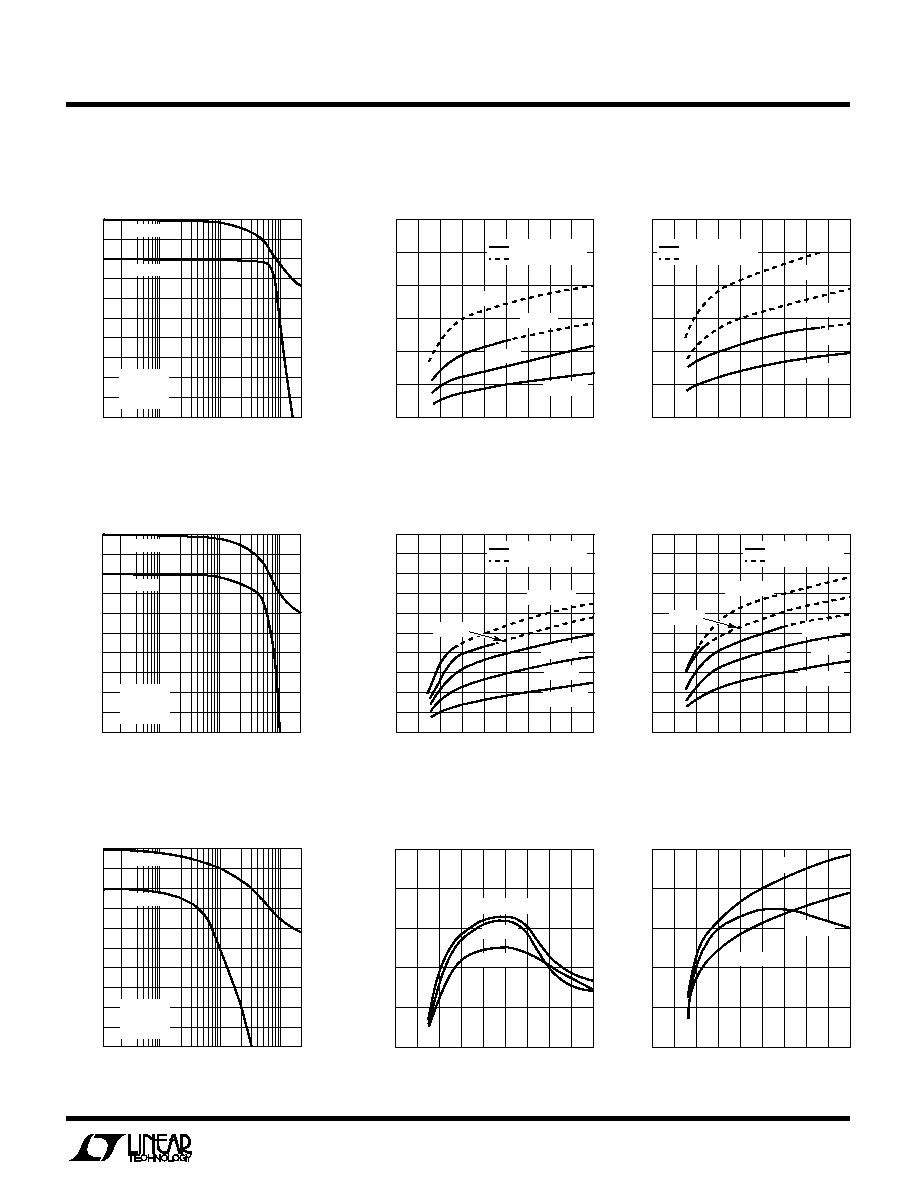
TYPICAL PERFOR
CE
Voltage Gain and Phase vs
3dB Bandwidth vs Supply
3dB Bandwidth vs Supply
Frequency, Gain = 40dB
Voltage, Gain = 100, R
L
= 100
Voltage, Gain = 100, R
L
= 1k
Voltage Gain and Phase vs
3dB Bandwidth vs Supply
3dB Bandwidth vs Supply
Frequency, Gain = 6dB
Voltage, Gain = 2, R
L
= 100
Voltage, Gain = 2, R
L
= 1k
Voltage Gain and Phase vs
3dB Bandwidth vs Supply
3dB Bandwidth vs Supply
Frequency, Gain = 20dB
Voltage, Gain = 10, R
L
= 100
Voltage, Gain = 10, R
L
= 1k
SUPPLY VOLTAGE (
±
V)
0
0
3dB BANDWIDTH (MHz)
0.5
1.0
1.5
2.0
2.5
4
8
14
18
LT1217 · TPC09
2
6
10
12
16
R
F
= 250
R
F
= 5.1k
R
F
= 1k
SUPPLY VOLTAGE (
±
V)
0
0
3dB BANDWIDTH (MHz)
5
10
15
20
25
30
4
8
14
18
LT1217 · TPC03
2
6
10
12
16
R
F
= 1k
R
F
= 2k
R
F
= 3k
R
F
= 5.1k
PEAKING
0.5dB
PEAKING
5dB
SUPPLY VOLTAGE (
±
V)
0
0
3dB BANDWIDTH (MHz)
4
6
12
16
18
20
4
8
14
18
LT1217 · TPC06
2
6
10
12
16
R
F
= 5.1k
14
10
8
2
PEAKING
0.5dB
PEAKING
5dB
R
F
= 2k
R
F
= 3k
R
F
= 1k
R
F
= 750
FREQUENCY (MHz)
0.01
2
VOLTAGE GAIN (dB)
1
5
7
8
0.1
1.0
10
LT1217 · TPC01
1
0
2
3
4
6
135
45
0
225
180
90
PHASE SHIFT (DEGREES)
V
S
=
±
15V
R
L
= 100
R
F
= 3k
PHASE
GAIN
FREQUENCY (MHz)
0.01
32
VOLTAGE GAIN (dB)
35
39
41
42
0.1
1.0
10
LT1217 · TPC07
33
34
36
37
38
40
135
45
0
225
180
90
PHASE SHIFT (DEGREES)
PHASE
GAIN
V
S
=
±
15V
R
L
= 100
R
F
= 3k
FREQUENCY (MHz)
0.01
12
VOLTAGE GAIN (dB)
15
19
21
22
0.1
1.0
10
LT1217 · TPC04
13
14
16
17
18
20
135
45
0
225
180
90
PHASE SHIFT (DEGREES)
V
S
=
±
15V
R
L
= 100
R
F
= 3k
PHASE
GAIN
SUPPLY VOLTAGE (
±
V)
0
0
3dB BANDWIDTH (MHz)
5
10
15
20
25
30
4
8
14
18
LT1217 · TPC02
2
6
10
12
16
R
F
= 1k
R
F
= 2k
R
F
= 3k
R
F
= 5.1k
PEAKING
0.5dB
PEAKING
5dB
SUPPLY VOLTAGE (
±
V)
0
0
3dB BANDWIDTH (MHz)
4
6
12
16
18
20
4
8
14
18
LT1217 · TPC05
2
6
10
12
16
R
F
= 5.1k
14
10
8
2
PEAKING
0.5dB
PEAKING
5dB
R
F
= 2k
R
F
= 3k
R
F
= 1k
R
F
= 750
SUPPLY VOLTAGE (
±
V)
0
0
3dB BANDWIDTH (MHz)
0.5
1.0
1.5
2.0
2.5
4
8
14
18
LT1217 · TPC08
2
6
10
12
16
R
F
= 250
R
F
= 5.1k
R
F
= 1k
LT1217
4
C
C
HARA TERISTICS
U
W
A
TYPICAL PERFOR
CE
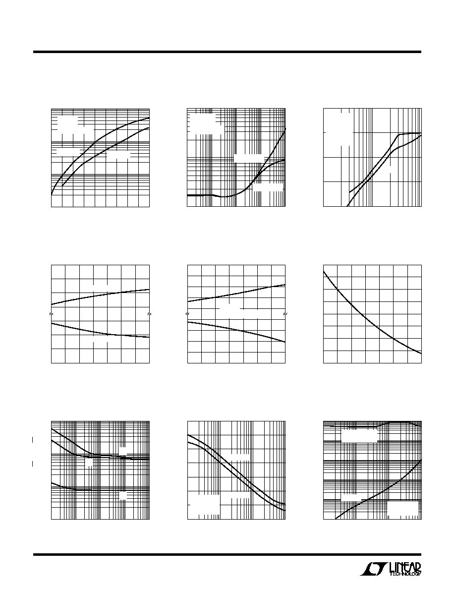
Maximum Capacitive Load vs
Total Harmonic Distortion vs
2nd and 3rd Harmonic
Feedback Resistor
Frequency
Distortion vs Frequency
Input Common Mode Limit vs
Output Saturation Voltage vs
Output Short Circuit Current vs
Temperature
Temperature
Temperature
Spot Noise Voltage and Current vs
Power Supply Rejection vs
Output Impedance vs
Frequency
Frequency
Frequency
PACKAGE TEMPERATURE (°C)
50
V
COMMON MODE RANGE (V)
1.0
2.0
3.0
2.0
1.0
V+
0
25
75
125
LT1217 · TPC13
25
50
100
3.0
V+ = +5V TO +18V
V = 5V TO 18V
PACKAGE TEMPERATURE (°C)
50
V
OUTPUT SATURATION VOLTAGE (V) 0.5
1.5
2.0
1.5
1.0
V+
0
25
75
125
LT1217 · TPC14
25
50
100
2.0
1.0
0.5
R
L
=
±
5V
V
S
±
18V
FREQUENCY (MHz)
0.01
0.1
RESISTANCE (
)
1
100
1000
10000
0.1
1
10
LT1217 · TPC18
V
S
=
±
15V
R
F
= R
G
= 3k
10
NORMAL
SHUTDOWN
(PIN 8 AT GND)
FREQUENCY (MHz)
0.01
0
POWER SUPPLY REJECTION (dB)
20
50
60
70
0.1
1
10
LT1217 · TPC17
10
30
40
POSITIVE
NEGATIVE
V
S
=
±
15V
R
L
= 100
R
F
= R
G
=3k
PACKAGE TEMPERATURE (°C)
50
40
OUTPUT SHORT CIRCUIT CURRENT (mA)
50
70
90
100
120
0
25
75
125
LT1217 · TPC15
25
50
100
80
60
110
FREQUENCY (MHz)
0.1
60
DISTORTION (dBc)
50
40
30
20
1
10
LT1217 · TPC12
V
S
=
±
15V
R
L
= 100
V
O
= 2Vpp
R
F
= 3k
A
V
= 10dB
3RD
2ND
FEEDBACK RESISTOR (k
)
1
10
CAPACITIVE LOAD (pF)
100
1000
10000
4
7
10
LT1217 · TPC10
2
3
5
6
8
9
A
V
= 2
R
L
= 1k
PEAKING
5dB
V
S
=
±
5V
V
S
=
±
15V
FREQUENCY (kHz)
SPOT NOISE (nV/
Hz OR pA/
Hz)
1
10
100
0.01
1
10
100
LT1217 · TPC16
0.1
0.1
e
n
i
n
i
n+
FREQUENCY (Hz)
TOTAL HARMONIC DISTORTION (%)
0.01
0.1
10
1000
10000
100000
LT1217 · TPC11
0.001
100
V
S
=
±
15V
R
L
= 400
R
F
= R
G
= 3k
V
O
= 7V
RMS
V
O
= 2V
RMS
5
LT1217
C
C
HARA TERISTICS
U
W
A
TYPICAL PERFOR
CE
Settling Time to 10mV vs
Settling Time to 1mV vs
Output Step
Output Step
Supply Current vs Supply Voltage
SETTLING TIME (ns)
0
10
OUTPUT STEP (V)
6
4
0
4
6
10
200
400
500
LT1217 · TPC20
300
8
2
2
8
100
NON-INVERTING
INVERTING
NON-INVERTING
INVERTING
V
S
=
±
15V
R
F
= R
G
= 3k
SUPPLY VOLTAGE (
±
V)
0
0.0
SUPPLY CURRENT (mA)
0.2
0.4
0.6
1.0
1.2
1.4
4
10
14
18
LT1217 · TPC21
2
6
8
12
16
0.8
T = 25°C, 125°C
T = 55°C
T = 25°C
T = 125°C
SHUTDOWN
PIN 8 AT GND
T = 55°C
SETTLING TIME (ns)
0
10
OUTPUT STEP (V)
6
4
0
4
6
10
100
150
250
300
LT1217 · TPC19
50
200
8
2
2
8
INVERTING
NON-INVERTING
V
S
=
±
15V
R
F
= R
G
= 3k
NON-INVERTING
INVERTING
U
S
A
O
PPLICATI
W
U
U
I FOR ATIO
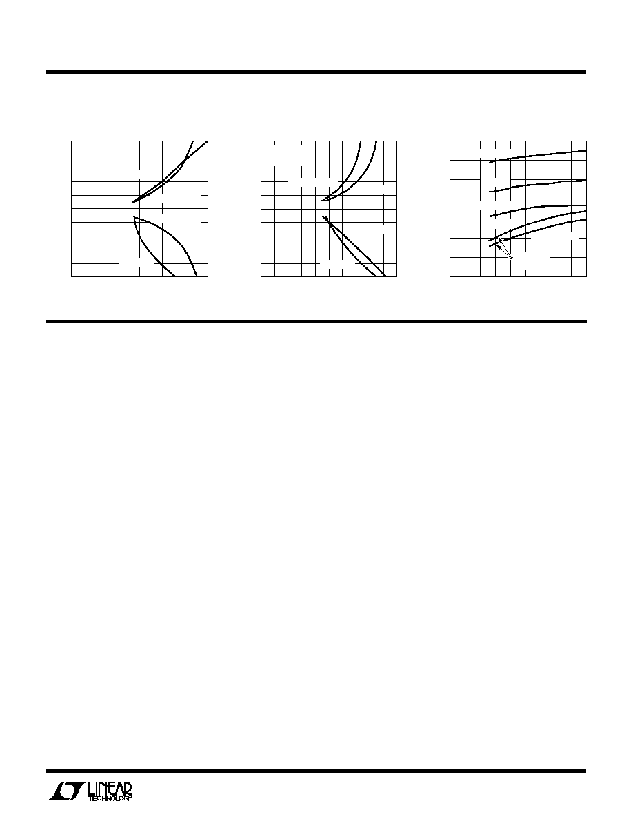
Current Feedback Basics
The small signal bandwidth of the LT1217, like all current
feedback amplifiers, isn't a straight inverse function of the
closed loop gain. This is because the feedback resistors
determine the amount of current driving the amplifier's
internal compensation capacitor. In fact, the amplifier's
feedback resistor (R
F
) from output to inverting input
works with internal junction capacitances of the LT1217 to
set the closed loop bandwidth.
Even though the gain set resistor (R
G
) from inverting input
to ground works with R
F
to set the voltage gain just like it
does in a voltage feedback op amp, the closed loop
bandwidth does not change. This is because the equivalent
gain bandwidth product of the current feedback amplifier
is set by the Thevenin equivalent resistance at the inverting
input and the internal compensation capacitor. By keeping
R
F
constant and changing the gain with R
G
, the Thevenin
resistance changes by the same amount as the change in
gain. As a result, the net closed loop bandwidth of the
LT1217 remains the same for various closed loop gains.
The curve on the first page shows the LT1217 voltage gain
versus frequency while driving 100
, for five gain settings
from 1 to 100. The feedback resistor is a constant 3k and
the gain resistor is varied from infinity to 30
. Second
order effects reduce the bandwidth somewhat at the
higher gain settings.
Feedback Resistor Selection
The small signal bandwidth of the LT1217 is set by the
external feedback resistors and the internal junction ca-
pacitors. As a result, the bandwidth is a function of the
supply voltage, the value of the feedback resistor, the
closed loop gain and load resistor. The characteristic
curves of bandwidth versus supply voltage are done with
a heavy load (100
) and a light load (1k
) to show the
effect of loading. These graphs also show the family of
curves that result from various values of the feedback
resistor. These curves use a solid line when the response
has less than 0.5dB of peaking and a dashed line when the
response has 0.5dB to 5dB of peaking. The curves stop
where the response has more than 5dB of peaking.
At a gain of two, on
±
15V supplies with a 3k
feedback
resistor, the bandwidth into a light load is 13.5MHz with a
little peaking, but into a heavy load the bandwidth is
10MHz with no peaking. At very high closed loop gains, the
bandwidth is limited by the gain bandwidth product of
about 100MHz. The curves show that the bandwidth at a
closed loop gain of 100 is about 1MHz.
Capacitance on the Inverting Input
Current feedback amplifiers want resistive feedback from
the output to the inverting input for stable operation. Take