 | ÐлекÑÑоннÑй компоненÑ: LT1239 | СкаÑаÑÑ:  PDF PDF  ZIP ZIP |
Äîêóìåíòàöèÿ è îïèñàíèÿ www.docs.chipfind.ru
1
LT1239
Backup Battery
Management Circuit
s
Micropower Operation (I
Q
= 20
µ
A)
s
Adjustable Regulator for Battery Charging
s
4.85V Regulator for Battery Regulation
s
Cell Voltage Equalization in 2-Cell Systems
s
Low-Battery Detector Protects Lithium Cells
s
Comparator for Automatic Power Switching
s
Shutdown
s
Output Current Sensing
s
Current and Thermal Limiting
s
Reverse Output Protection
s
16-Pin SO Package
s
Operates on 7V to 30V Input
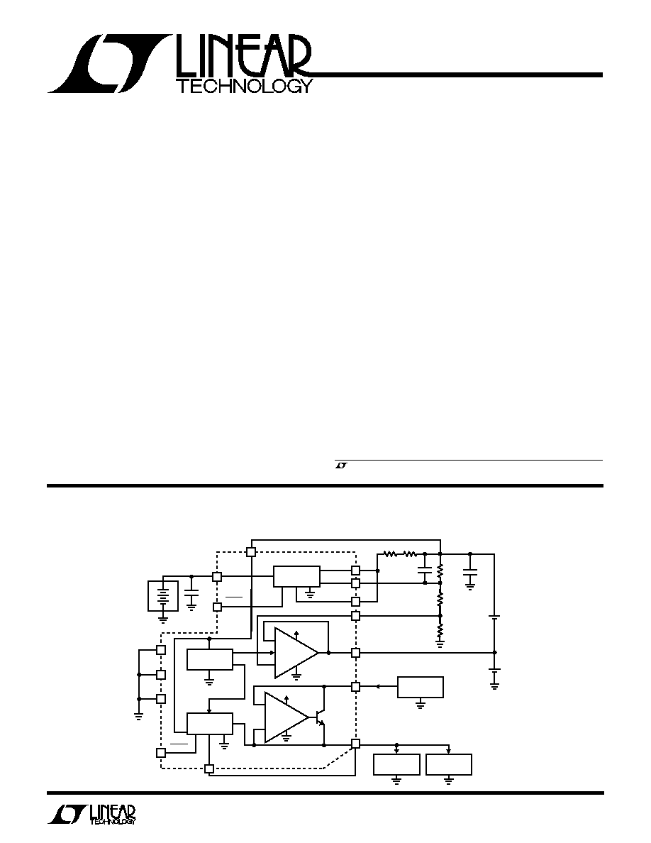
The LT
®
1239 is a micropower backup battery manage-
ment system for portable computers and instrumenta-
tion. It contains two regulators for regulating the battery
voltage and memory voltage and a comparator for switch-
ing between main power and backup power. The first
regulator provides a constant voltage charge for the
backup batteries and is adjustable from 3.75V up to 20V.
An equalization amplifier combined with the first regulator
provides precision charge equalization for a 2-cell
lithium-ion system. A second regulator with 4.85V output
provides a regulated backup battery voltage to the memory
when main power is lost. The second regulator also
isolates the backup battery from the main 5V supply
during normal operation when the memory is being pow-
ered by the 5V supply.
A comparator is included which provides automatic
switchover from main 5V power to backup power ensur-
ing uninterrupted power for memory and power monitor-
FEATURES
DESCRIPTIO
N
U
s
Backup Battery Management Systems for Portable
Computers
s
Lithium-Ion Backup Systems
s
NiCd Backup Systems
APPLICATIO
N
S
U
TYPICAL APPLICATIO
N
U
, LTC and LT are registered trademarks of Linear Technology Corporation.
Lithium-Ion Backup System
604k
1%
69.8k
1%
681k
1%
22
µ
F
3.4V
Li-Ion
CELL
3.4V
Li-Ion
CELL
E/A (IN)
E/A (OUT)
5V
IN
OUT 1
ADJ
I
MON1
300pF
INPUT 2
120
* 120
*
INPUT 2
OUT 2
I
MON2
SHDN1
IN
MAIN
BATTERY
PACK
7V TO 24V
INPUT 1
22
µ
F
INPUT 1
SHDN2
OUT
IN
GND
GND
GND
GND
GND
* REQUIRED BY SOME SAFETY AGENCIES
SEE APPLICATIONS INFORMATION
FOR INFORMATION ON
SELECTING VALUES.
LTC1239 · TA01
+
+
5V SYSTEM
POWER
MEMORY
POWER
MANAGEMENT
LOW-BATTERY
DETECT
+
+
11
1
7
8
15
16
13
12
10
2
4
5
6
14
3
REGULATOR
#1
REGULATOR
#2
2
LT1239
DESCRIPTIO
N
U
ing circuitry. A low-battery detector with a 5V threshold
powers down the second regulator and the error amplifier
to limit the discharge voltage of the backup cells. This
prevents deep discharge damage to the lithium cells. Both
regulators have independent shutdown and current moni-
tor functions.
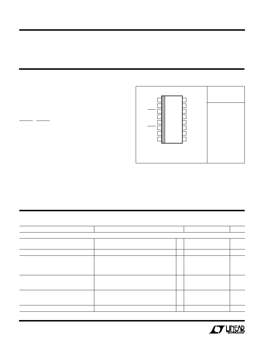
LT1239CS
ORDER PART
NUMBER
Consult factory for Industrial and Military grade parts.
T
JMAX
= 100
°
C,
JA
= 120
°
C/ W
PARAMETER
CONDITIONS
MIN
TYP
MAX
UNITS
Regulator 1 (Notes 7, 8)
Regulated Output Voltage (V
ADJ
= V
OUT1
)
V
IN1
= 4.3V, I
OUT
= 1mA, T
J
= 25
°
C
3.700
3.750
3.800
V
V
IN1
= 4.8V to 24V, I
OUT
= 1mA to 30mA
q
3.650
3.750
3.825
V
Line Regulation
I
LOAD
= 1mA, V
IN1
= 4.3V to 30V
q
2
10
mV
Load Regulation
V
IN1
= 5V, I
LOAD
= 1mA to 30mA, T
J
= 25
°
C
12
25
mV
V
IN1
= 5V, I
LOAD
= 1mA to 30mA
q
20
50
mV
V
IN1
= 5V, I
LOAD
= 1mA to 50mA, T
J
= 25
°
C
20
mV
V
IN1
= 5V, I
LOAD
= 1mA to 50mA
30
mV
Dropout Voltage (Note 9)
I
LOAD
= 1mA, T
J
= 25
°
C
0.15
0.20
V
I
LOAD
= 30mA, T
J
= 25
°
C
0.25
0.40
V
I
LOAD
= 50mA, T
J
= 25
°
C
0.30
V
Ground Pin Current (Notes 10, 11)
I
LOAD
= 0mA, V
IN1
= 3.75V
q
20
30
µ
A
I
LOAD
= 30mA, V
IN1
= 3.75V
q
0.80
1.2
mA
I
LOAD
= 50mA, V
IN1
= 3.75V
1.35
mA
Adjust Pin Bias Current (Note 12)
T
J
= 25
°
C
40
120
nA
ELECTRICAL CHARACTERISTICS
PACKAGE/ORDER I
N
FOR
M
ATIO
N
W
U
U
(Note 1)
Input 1 Voltage ......................................................
±
30V
Input 2 Voltage ............................................. 30V, 0.6V
Output 1 Voltage ........................................... 30V, 0.6V
Output 2 Voltage ............................................. 6V, 0.6V
Adjust Pin Current ................................................ 10mA
SHDN1, SHDN2 (Note 2)
Input Voltage .............................................. 6V, 0.6V
Input Current ...................................................... 5mA
I
MON1
Voltage
(Note 3) .......................... (V
IN1
30V) < I
MON1
< V
IN1
I
MON2
Voltage
(Note 4) .......................... (V
IN2
30V) < I
MON2
< V
IN2
E/A Output Voltage (Note 5) .... 0.6V < V
E/A(OUT)
< V
IN2
E/A Input Voltage (Note 5) .......... 0.6V < V
E/A(IN)
< V
IN2
5V Input Voltage ............................................. 6V, 0.6V
Operating Temperature Range ......................... 0 to 70
°
C
Junction Temperature Range ............................. (Note 6)
Storage Temperature Range ................. 65
°
C to 150
°
C
Lead Temperature (Soldering, 10 sec) .................. 300
°
C
ABSOLUTE
M
AXI
M
U
M
RATINGS
W
W
W
U
TOP VIEW
S PACKAGE
16-LEAD PLASTIC SO
1
2
3
4
5
6
7
8
16
15
14
13
12
11
10
9
ADJ
GND
SHDN1
GND
GND
SHDN2
E/A (IN)
E/A (OUT)
OUT 1
I
MON1
INPUT 1
5V
IN
OUT 2
I
MON2
INPUT 2
NC
3
LT1239
ELECTRICAL CHARACTERISTICS
PARAMETER
CONDITIONS
MIN
TYP
MAX
UNITS
Regulator 1 (Notes 7, 8)
Shutdown Threshold
V
OUT1
= Off to On
q
1.20
2.8
V
V
OUT1
= On to Off
q
0.25
0.75
V
Shutdown Pin Current (Note 13)
V
SHDN1
= 0V
q
2
4
µ
A
Quiescent Current in Shutdown (Note 10)
V
IN1
= 24V, V
SHDN1
= 0V
q
10
16
µ
A
Ripple Rejection
V
IN1
= 5V (Avg), V
RIPPLE
= 0.5V
P-P
f
RIPPLE
= 120Hz, I
LOAD
= 20mA, T
J
= 25
°
C
50
59
dB
Current Limit
V
IN1
= 7V, V
OUT1
= 0V, T
J
= 25
°
C
30
50
mA
V
OUT1
= V
OUT1(NOM)
100mV, T
J
= 25
°
C
40
70
mA
Reverse Output Current
V
OUT1
= 3.75V, V
IN1
< 3.75V
q
6
12
µ
A
V
OUT1
= 3.75V, V
IN1
= Open Circuit
q
6
12
µ
A
Current Monitor Pin Output Current
V
OUT1
= 3.75V, V
IMON1
= 0V, I
OUT1
= 1mA
4.6
µ
A
V
OUT1
= 3.75V, V
IMON1
= 0V, I
OUT1
= 10mA
q
38
44
50
µ
A
V
OUT1
= 3.75V, V
IMON1
= 0V, I
OUT1
= 50mA
215
µ
A
Comparator
Output Saturation Voltage (V
5VIN
V
OUT2
)
V
IN1
= 7V, V
IN2
= 0V, V
5VIN
= 5V, I
OUT2
= 1mA
q
12
40
mV
V
IN1
= 7V, V
IN2
= 0V, V
5VIN
= 5V, I
OUT2
= 30mA
q
110
150
mV
V
IN1
= 7V, V
IN2
= 0V, V
5VIN
= 5V, I
OUT2
= 50mA
q
135
220
mV
Low-Battery Detector
Turn-Off Threshold
T
J
= 25
°
C
4.85
5.00
5.15
V
Turn-On Threshold
T
J
= 25
°
C
5.3
V
Hysteresis
T
J
= 25
°
C
0.2
0.3
V
Regulator 2
Regulated Output Voltage
V
IN2
= 6.8V, I
OUT
= 1mA, T
J
= 25
°
C
4.775
4.850
4.925
V
Output Voltage Temperature Coefficient
0.5
mV/
°
C
Line Regulation
I
OUT2
= 1mA, V
IN2
= 5.4V to 10V
q
2
5
mV
Load Regulation
V
IN2
= 6.8V, I
LOAD
= 1mA to 30mA, T
J
= 25
°
C
12
25
mV
V
IN2
= 6.8V, I
LOAD
= 1mA to 30mA
q
20
50
mV
V
IN2
= 6.8V, I
LOAD
= 1mA to 50mA, T
J
= 25
°
C
20
mV
V
IN2
= 6.8V, I
LOAD
= 1mA to 50mA
30
mV
Ground Pin Current
I
LOAD
= 0mA, V
IN2
= 5.4V
q
16
25
µ
A
I
LOAD
= 30mA, V
IN2
= 5.4V
q
0.80
1.2
mA
I
LOAD
= 50mA, V
IN2
= 5.4V
q
1.35
mA
Shutdown Threshold
V
OUT2
= Off to On
q
1.20
2.8
V
V
OUT2
= On to Off
q
0.25
0.75
V
Shutdown Pin Current
V
SHDN2
= 0V
q
1.7
4
µ
A
Ripple Rejection
V
IN2
= 6.4V (Avg), V
RIPPLE
= 0.5V
P-P
f
RIPPLE
= 120Hz, I
LOAD
= 20mA, T
J
= 25
°
C
50
58
dB
Current Limit
V
IN2
= 6.8V, V
OUT2
= 0V, T
J
25
°
C
30
50
mA
V
OUT2
= V
OUT2(NOM)
100mV, T
J
= 25
°
C
40
70
mA
Reverse Output Current
V
OUT2
= 4.85V, V
IN2
< 4.85V
q
6
12
µ
A
V
OUT2
= 4.85V, V
IN2
= Open Circuit
q
6
12
µ
A
Current Monitor Pin Output Current
V
OUT2
= 6.8V, V
IMON2
= 0V, I
OUT2
= 1mA
4.7
µ
A
V
OUT2
= 6.8V, V
IMON2
= 0V, I
OUT2
= 10mA
q
35
41
47
µ
A
V
OUT2
= 6.8V, V
IMON2
= 0V, I
OUT2
= 50mA
210
µ
A
Error Amplifier
Bias Current
V
E/A(IN)
= 3.4V, V
IN2
= 6.8V
q
3
20
nA
4
LT1239
ELECTRICAL CHARACTERISTICS
PARAMETER
CONDITIONS
MIN
TYP
MAX
UNITS
Offset Voltage
q
0
15
mV
Output Current Sourcing
V
IN2
= 6.8V, V
E/A(IN)
= 3.4V, T
J
= 25
°
C
3
5
mA
Sinking
V
IN2
= 6.8V, V
E/A(IN)
= 3.4V, T
J
= 25
°
C
3
5
mA
Regulator 2, Low Battery Detector and Error Amplifier
Quiescent Current
V
IN2
= 6.8V, 5V
IN
= 0V, V
E/A(IN)
= 3.4V
q
20
30
µ
A
V
IN2
= 6.8V, 5V
IN
= 0V, V
E/A(IN)
= 3.4V, V
PIN6
= 0V
q
8
12
µ
A
V
IN2
= 4.8V, 5V
IN
= 0V, V
E/A(IN)
= 2.4V
q
3
6
µ
A
The
q
denotes specifications which apply over the full operating
temperature range.
Note 1: All voltages are with respect to the ground pins of the device
(pins 2, 4, 5) unless otherwise specified.
Note 2: The shutdown pin input voltage rating is required for a low
impedance source. Internal protection devices connected to the shutdown
pin will turn on and clamp the pin to approximately 7V or 0.6V. This
range allows the use of 5V logic devices to drive the pin directly. For high
impedance sources or logic running on supply voltages greater than 5.5V,
the maximum current driven into the shutdown pin must be limited to
5mA.
Note 3: The current monitor pin for regulator 1 (pin 15) can be pulled 30V
below the input pin (pin 14). The current monitor pin must not be pulled
above the input pin.
Note 4: The current monitor pin for regulator 2 (pin 11) can be pulled 30V
below the input pin (pin 10). The current monitor pin must not be pulled
above the input pin.
Note 5: E/A (OUT) pin should not be pulled below ground or above
the voltage at Input 2.
Note 6: The device is specified to an operating temperature range of 0
°
C to
70
°
C. The device is guaranteed to be functional up to the thermal
shutdown temperature. The thermal shutdown temperature for this device
is approximately 100
°
C.
Note 7: Operating conditions are limited by maximum junction
temperature. The regulated output specification will not apply for all
possible combinations of input voltage and output current. When
operating at maximum output current, the input voltage range must be
limited. When operating at maximum input voltage, the output current
range must be limited.
Note 8: Regulator 1 of the LT1239 is tested and specified with the adjust
pin (pin 1) tied to the output pin (pin 16). See Applications Information.
Note 9: Dropout voltage is the minimum input/output voltage required to
maintain regulation at the specified output current. In dropout, the output
voltage measured at the package pins will be equal to (V
IN
V
DROPOUT
).
Note 10: The quiescent current of the comparator is included in the
ground pin current and quiescent current specifications for regulator 1.
The comparator output is turned off (pin 13 = 0V, pin 12 = 5V) during
these tests.
Note 11: Ground pin current for regulator 1 is tested with V
IN
= V
OUT
(nominal) and a current source load. This means that the device is tested
in it's dropout region. Ground pin current will decrease slightly at higher
input voltages.
Note 12: Adjust pin current flows into the adjust pin.
Note 13: Shutdown pin current at V
SHDN
= 0V flows out of
the shutdown pin.
Note 14: 6.8V is the nominal voltage of two lithium-ion cells.
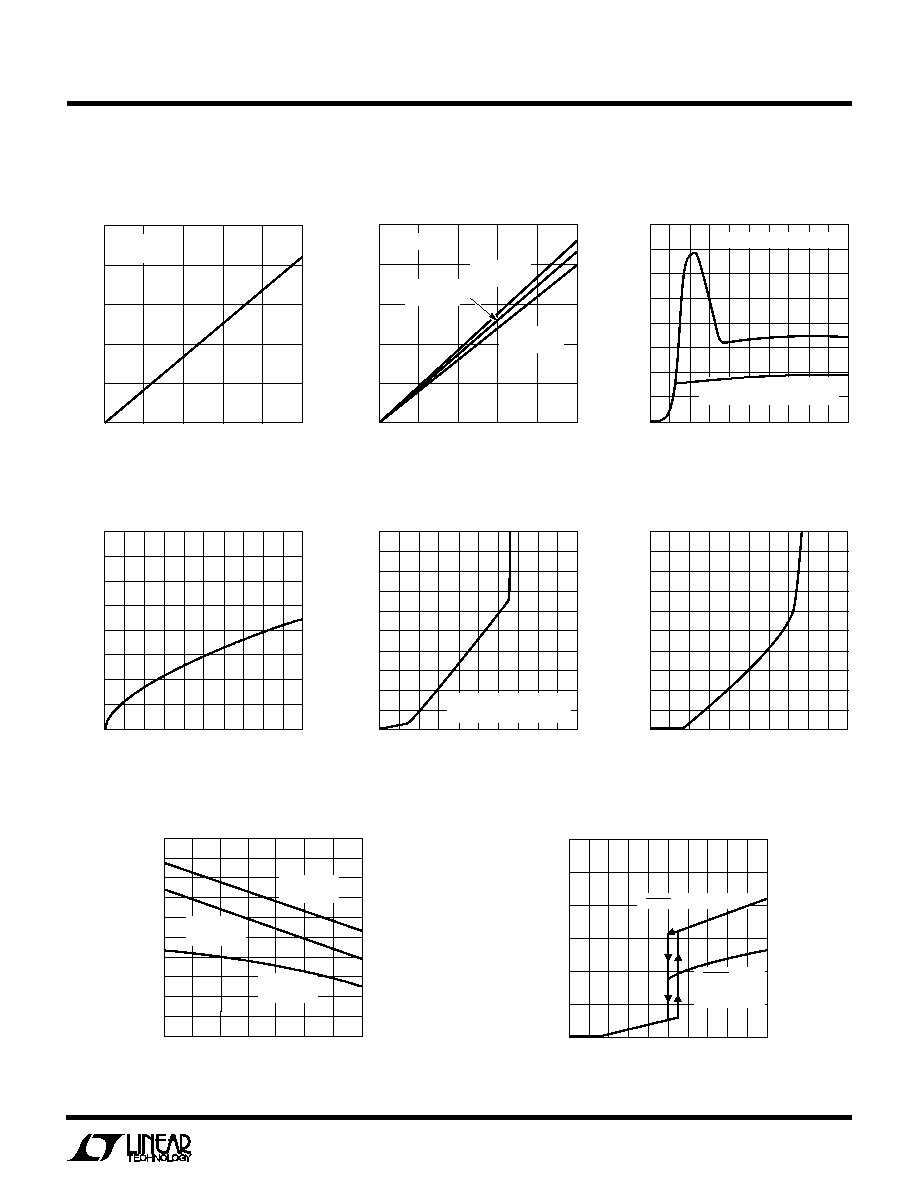
TYPICAL PERFOR
M
A
N
CE CHARACTERISTICS
U
W
Low-Battery Detector Thresholds
vs Temperature
Regulator 2 Output Voltage vs
Temperature
Regulator 1 Adjust Pin Voltage vs
Temperature
TEMPERATURE (
°
C)
50
25
75
LT1239 · TPC01
25
0
50
100
LOW-BATTERY DETECTOR THRESHOLD (V)
5.60
5.50
5.40
5.30
5.20
5.10
5.00
4.90
START-UP THRESHOLD
SHUTDOWN THRESHOLD
TEMPERATURE (
°
C)
50
REGULATOR 2 OUTPUT VOLTAGE (V)
25
0
25
50
LT1239 · TPC02
75
4.975
4.950
4.925
4.900
4.875
4.850
4.825
4.800
4.775
4.750
4.725
100
TEMPERATURE (
°
C)
50
ADJUST PIN VOLTAGE (V)
25
0
25
50
LT1239 · TPC03
75
3.80
3.79
3.78
3.77
3.76
3.75
3.74
3.73
3.72
3.71
3.70
100
5
LT1239
TYPICAL PERFOR
M
A
N
CE CHARACTERISTICS
U
W
Regulator 1, Comparator Quiescent
Current vs Input Voltage, Pin 14
Regulator 1 I
MON
Current vs
Output Current
Regulator 2 I
MON2
Current vs
Output Current
OUTPUT CURRENT (mA)
0
I
MON2
CURRENT (
µ
A)
250
200
150
100
50
0
40
LT1239 · TPC04
10
20
30
50
V
IN2
= 6.8V
V
IMON2
= 0V
OUTPUT CURRENT (mA)
0
I
MON1
CURRENT (
µ
A)
250
200
150
100
50
0
40
LT1239 · TPC05
10
20
30
50
V
IMON1
= 0V
V
IN1
= 24V
V
OUT1
= 6.8V
V
IN1
= 5V
V
OUT1
= 3.75V
V
IN1
= 5V
V
OUT1
= 3.75V
INPUT VOLTAGE, PIN 14 (V)
0
QUIESCENT CURRENT (
µ
A)
40
35
30
25
20
15
10
5
0
LT1239 · TPC06
10
5
V
ADJ
(PIN 1) = V
OUT
(PIN 16)
V
PIN3
= 0V
(REGULATOR 1 IN SHUTDOWN)
Regulator 2 Reverse Output
Current vs Output Voltage
Regulator 1 Reverse Output
Current vs Output Voltage
Comparator Output Saturation
Voltage vs Output Current
TEMPERATURE (
°
C)
50
SHUTDOWN PIN THRESHOLD (V)
2.0
1.8
1.6
1.4
1.2
1.0
0.8
0.6
0.4
0.2
0
0
50
75
LT1239 · TPC10
25
25
100
125
(ON-TO-OFF)
I
LOAD
= 1mA
(OFF-TO-ON)
I
LOAD
= 1mA
(OFF-TO-ON)
I
LOAD
= 30mA
Regulator 2, Error Amp, Low-
Battery Detector Quiescent Current
INPUT 2 VOLTAGE, PIN 10 (V)
QUIESCENT CURRENT (
µ
A)
30
25
20
15
10
5
0
2
4
6
8
LT1239 · TPC11
10
1
0
3
5
7
9
V
SHDN2
= OPEN CIRCUIT
V
SHDN2
= 0V
(REGULATOR 2
IN SHUTDOWN)
Shutdown Pin Threshold
OUTPUT VOLTAGE (V)
0
REVERSE OUTPUT CURRENT (
µ
A)
20
18
16
14
12
10
8
6
4
2
0
8
LT1239 · TPC09
2
1
3
5
7
9
4
6
10
OUTPUT VOLTAGE (V)
0
REVERSE OUTPUT CURRENT (
µ
A)
20
18
16
14
12
10
8
6
4
2
0
8
LT1239 · TPC08
2
1
3
5
7
9
4
6
10
V
IN1
= 0V
ADJ (PIN 1) = V
OUT
(PIN 16)
OUTPUT CURRENT (mA)
0
OUTPUT SATURATION VOLTAGE (mV)
400
350
300
250
200
150
100
50
0
80
LT1239 · TPC07
20
40
60
100
70
10
30
50
90